AD7859/AD7859L
REV. A
–9–
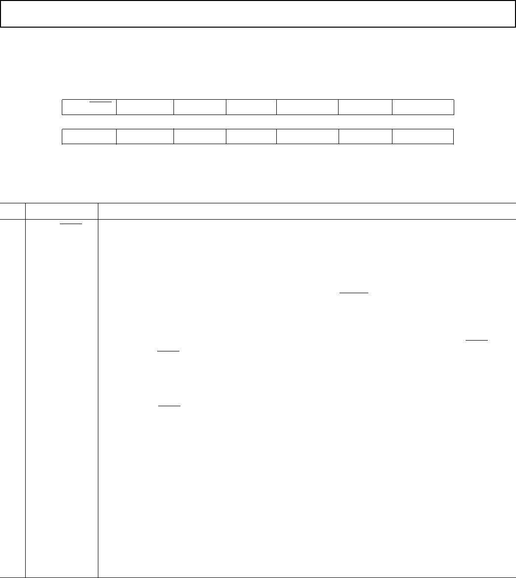
CONTROL REGISTER
The arrangement of the control register is shown below. The control register is a write only register and contains 14 bits of data. The
control register is selected by putting two 1s in ADDR1 and ADDR0. The function of the bits in the control register is described
below. The power-up status of all bits is 0.
MSB
SGL/DIFF CHSLT2 CHSLT1 CHSLT0 PMGT1 PMGT0 RDSLT1
RDSLT0 AMODE CONVST CALMD CALSLT1 CALSLT0 STCAL
LSB
CONTROL REGISTER BIT FUNCTION DESCRIPTION
Bit Mnemonic Comment
13 SGL/
DIFF A 0 in this bit position configures the input channels for pseudo-differential mode. A 1 in this bit posi-
tion configures the input channels in single ended mode. Please see Table III for channel selection.
12 CHSLT2 These three bits are used to select the analog input on which the conversion is performed. The analog
11 CHSLT1 inputs can be configured as eight single-ended channels or four pseudo-differential channels. The
10 CHSLT0 default selection is AIN1 for the positive input and AIN2 for the negative input. Please see Table III for
channel selection information.
9 PMGT1 Power Management Bits. These two bits are used with the
SLEEP pin for putting the part into various
8 PMGT0 Power-Down modes (See Power-Down section for more details).
7 RDSLT1 Theses two bits determine which register is addressed for the read operations. Please see Table II.
6 RDSLT0
5 AMODE Analog Mode Bit. This bit has two different functions, depending on the status of the SGL/
DIFF bit.
When SGL/
DIFF is 0, AMODE selects between unipolar and bipolar analog input ranges. A logic 0 in
this bit position selects the unipolar range, 0 to V
REF
(i.e., AIN(+) – AIN(–) = 0 to V
REF
). A logic 1 in
this bit position selects the bipolar range –V
REF
/2 to +V
REF
/2 (i.e., AIN(+) – AIN(–) = –V
REF
/2 to
+V
REF
/2). In this case AIN(–) needs to be tied to at least +V
REF
/2 to allow AIN(+) to have a full input
swing from 0 V to +V
REF
.
When SGL/
DIFF is 1, AMODE selects the source for the AIN(–) channel of the sample and hold cir-
cuitry. If AMODE is a 0, AGND is selected. If AMODE is a 1, then AIN8 is selected. Please see
Table III for more information.
4 CONVST Conversion Start Bit. A logic 1 in this bit position starts a single conversion, and this bit is automatically
reset to 0 at the end of conversion. This bit may also be used in conjunction with system calibration (see
calibration section on page 21).
3 CALMD Calibration Mode Bit. A 0 here selects self-calibration and a 1 selects a system calibration (see Table IV).
2 CALSLT1 Calibration Selection Bits 1 and 0. These bits have two functions, depending on the STCAL bit.
1 CALSLT0 With the STCAL bit set to 1, the CALSLT1 and CALSLT0 bits, along with the CALMD bit, deter-
mine the type of calibration performed by the part (see Table IV).
With the STCAL bit set to 0, the CALSLT1 and CALSLT0 bits are decoded to address the calibration
register for read/write of calibration coefficients (see Table V for more details).
0 STCAL Start Calibration Bit. When STCAL is set to a 1, a calibration is performed, as determined by the
CALMD, CALSLT1 and CALSLT0 bits. Please see Table IV. When STCAL is set to a zero, no cali-
bration is performed.