REV. A
–3–
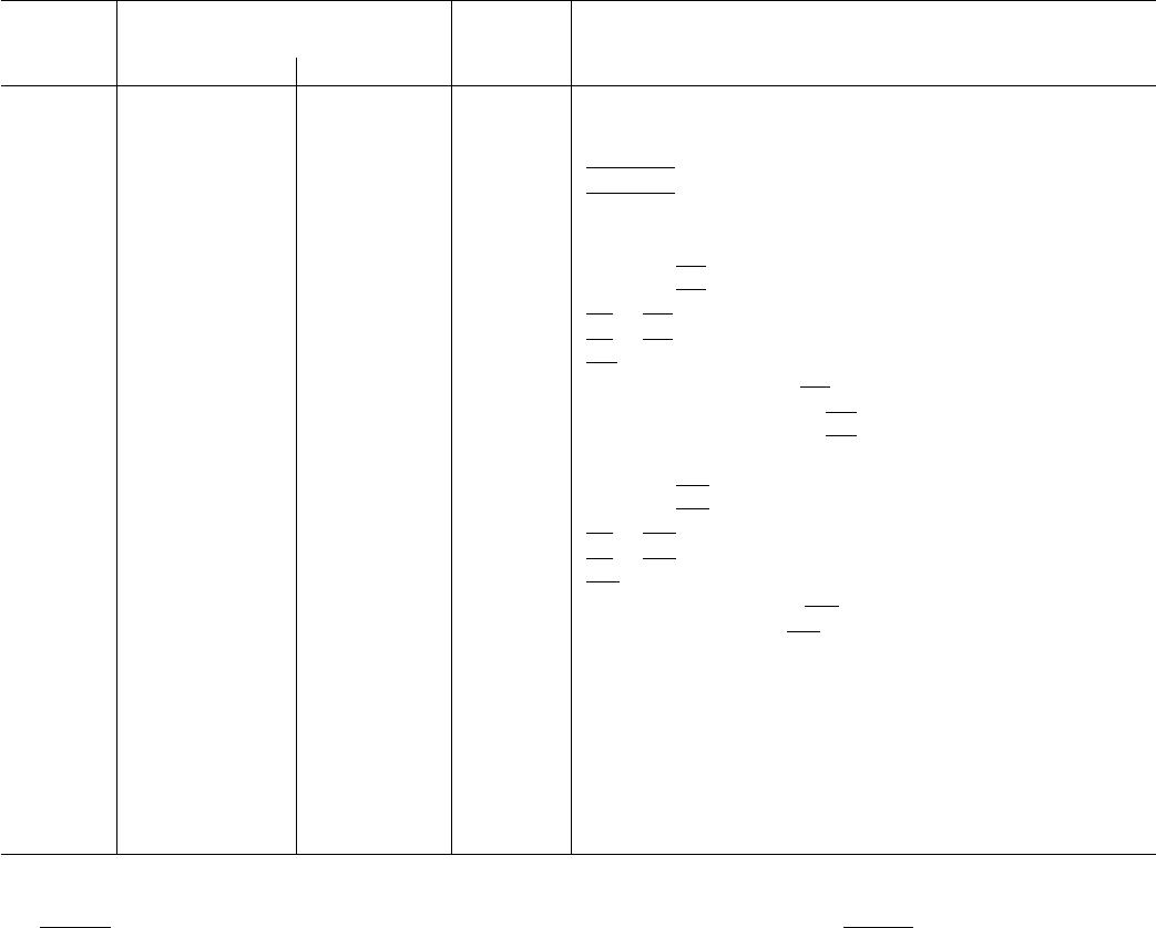
Parameter A Version
1
B Version
1
Units Test Conditions/Comments
CONVERSION RATE t
CLKIN
× 18
Conversion Time 4.5 (10) 4.5 µs max (L Versions Only, 0°C to +70°C, 1.8 MHz CLKIN)
Track/Hold Acquisition Time 0.5 (1) 0.5 µs min (L Versions Only, –40°C to +85°C, 1.8 MHz CLKIN)
POWER REQUIREMENTS
AV
DD,
DV
DD
+3.0/+5.5 +3.0/+5.5 V min/max
I
DD
Normal Mode
5
5.5 (1.95) 5.5 mA max AV
DD
= DV
DD
= 4.5 V to 5.5 V. Typically 4.5 mA
5.5 (1.95) 5.5 mA max AV
DD
= DV
DD
= 3.0 V to 3.6 V. Typically 4.0 mA
Sleep Mode
6
With External Clock On 10 10 µA typ Full Power-Down. Power Management Bits in Control
Register Set as PMGT1 = 1, PMGT0 = 0.
400 400 µA typ Partial Power-Down. Power Management Bits in
Control Register Set as PMGT1 = 1, PMGT0 = 1.
With External Clock Off 5 5 µA max Typically 1 µA. Full Power-Down. Power Management
Bits in Control Register Set as PMGT1 = 1, PMGT0 = 0.
200 200 µA typ Partial Power-Down. Power Management Bits in
Control Register Set as PMGT1 = 1, PMGT0 = 1.
Normal Mode Power Dissipation 30 (10) 30 (10) mW max V
DD
= 5.5 V: Typically 25 mW (8); SLEEP = V
DD
20 (6.5) 20 (6.5) mW max V
DD
= 3.6 V: Typically 15 mW (5.4); SLEEP = V
DD
Sleep Mode Power Dissipation
With External Clock On 55 55 µW typ V
DD
= 5.5 V; SLEEP = 0 V
36 36 µW typ V
DD
= 3.6 V; SLEEP = 0 V
With External Clock Off 27.5 27.5 µW max V
DD
= 5.5 V: Typically 5.5 µW; SLEEP = 0 V
18 18 µW max V
DD
= 3.6 V: Typically 3.6 µW; SLEEP = 0 V
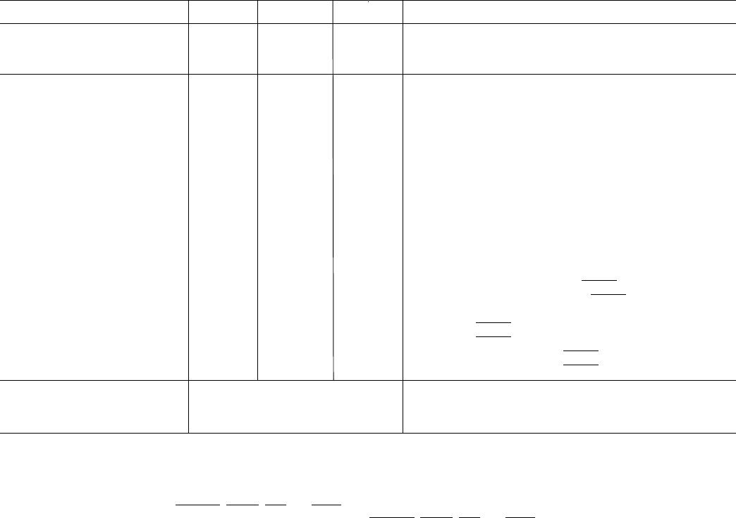
SYSTEM CALIBRATION
Offset Calibration Span
7
+0.05 × V
REF
/–0.05 × V
REF
V max/min Allowable Offset Voltage Span for Calibration
Gain Calibration Span
7
+1.025 × V
REF
/–0.975 × V
REF
V max/min Allowable Full-Scale Voltage Span for Calibration
NOTES
1
Temperature range as follows: A, B Versions, –40°C to +85°C.
2
Specifications apply after calibration.
3
SNR calculation includes distortion and noise components.
4
Not production tested, guaranteed by characterization at initial product release.
5
All digital inputs @ DGND except for CONVST, SLEEP, CAL, and SYNC @ DV
DD
. No load on the digital outputs. Analog inputs @ AGND.
6
CLKIN @ DGND when external clock off. All digital inputs @ DGND except for CONVST, SLEEP, CAL, and SYNC @ DV
DD
. No load on the digital outputs.
Analog inputs @ AGND.
7
The offset and gain calibration spans are defined as the range of offset and gain errors that the AD7859/AD7859L can calibrate. Note also that these are voltage spans
and are not absolute voltages (i.e., the allowable system offset voltage presented at AIN(+) for the system offset error to be adjusted out will be AIN(–) ±0.05 × V
REF
,
and the allowable system full-scale voltage applied between AIN(+) and AIN(–) for the system full-scale voltage error to be adjusted out will be V
REF
± 0.025 × V
REF
).
This is explained in more detail in the calibration section of the data sheet.
Specifications subject to change without notice.
AD7859/AD7859L
AD7859/AD7859L
REV. A
–4–
Limit at T
MIN
, T
MAX
(A, B Versions)
Parameter 5 V 3 V Units Description
f
CLKIN
2
500 500 kHz min Master Clock Frequency
4 4 MHz max
1.8 1.8 MHz max L Version
t
1
3
100 100 ns min CONVST Pulse Width
t
2
50 90 ns max CONVST to BUSY Propagation Delay
t
CONVERT
4.5 4.5 µs max Conversion Time = 18 t
CLKIN
10 10 µs max L Version 1.8 MHz CLKIN. Conversion Time = 18 t
CLKIN
t
3
15 15 ns min HBEN to RD Setup Time
t
4
5 5 ns min HBEN to RD Hold Time
t
5
0 0 ns min CS to RD to Setup Time
t
6
0 0 ns min CS to RD Hold Time
t
7
55 55 ns min RD Pulse Width
t
8
4
50 50 ns max Data Access Time After RD
t
9
5
5 5 ns min Bus Relinquish Time After RD
40 40 ns max Bus Relinquish Time After
RD
t
10
60 70 ns min Minimum Time Between Reads
t
11
0 0 ns min HBEN to WR Setup Time
t
12
5 5 ns max HBEN to WR Hold Time
t
13
0 0 ns min CS to WR Setup Time
t
14
0 0 ns max CS to WR Hold Time
t
15
55 70 ns min WR Pulse Width
t
16
10 10 ns min Data Setup Time Before WR
t
17
5 5 ns min Data Hold Time After WR
t
18
4
1/2 t
CLKIN
1/2 t
CLKIN
ns min New Data Valid Before Falling Edge of BUSY
t
19
2.5 t
CLKIN
2.5 t
CLKIN
ns max CS to BUSYin Calibration Sequence
t
CAL
6
31.25 31.25 ms typ Full Self-Calibration Time, Master Clock Dependent (125013
t
CLKIN
)
t
CAL1
6
27.78 27.78 ms typ Internal DAC Plus System Full-Scale Cal Time, Master Clock
Dependent (111124 t
CLKIN
)
t
CAL2
6
3.47 3.47 ms typ System Offset Calibration Time, Master Clock Dependent
(13889 t
CLKIN
)
NOTES
1
Sample tested at +25°C to ensure compliance. All input signals are specified with tr = tf = 5 ns (10% to 90% of V
DD
) and timed from a voltage level of 1.6 V.
2
Mark/Space ratio for the master clock input is 40/60 to 60/40.
3
The CONVST pulse width will here only apply for normal operation. When the part is in power-down mode, a different CONVST pulse width will apply (see Power-
Down section).
4
Measured with the load circuit of Figure 1 and defined as the time required for the output to cross 0.8 V or 2.4 V.
5
t
9
is derived form the measured time taken by the data outputs to change 0.5 V when loaded with the circuit of Figure 1. The measured number is then extrapolated
back to remove the effects of charging or discharging the 50 pF capacitor. This means that the time, t
9
, quoted in the timing characteristics is the true bus relinquish
time of the part and is independent of the bus loading.
6
The typical time specified for the calibration times is for a master clock of 4 MHz. For the L version the calibration times will be longer than those quoted here due to
the 1.8 MHz master clock.
Specifications subject to change without notice.
TIMING SPECIFICATIONS
1
(AV
DD
= DV
DD
= +3.0 V to +5.5 V; f
CLKIN
= 4 MHz for AD7859 and 1.8 MHz for AD7859L;
T
A
= T
MIN
to T
MAX
, unless otherwise noted)
AD7859/AD7859L
REV. A
–5–
ABSOLUTE MAXIMUM RATINGS
1
(T
A
= +25°C unless otherwise noted)
AV
DD
to AGND . . . . . . . . . . . . . . . . . . . . . . . . –0.3 V to +7 V
DV
DD
to DGND . . . . . . . . . . . . . . . . . . . . . . . –0.3 V to +7 V
AV
DD
to DV
DD
. . . . . . . . . . . . . . . . . . . . . . . –0.3 V to +0.3 V
Analog Input Voltage to AGND . . . . –0.3 V to AV
DD
+ 0.3 V
Digital Input Voltage to DGND . . . . –0.3 V to DV
DD
+ 0.3 V
Digital Output Voltage to DGND . . . –0.3 V to DV
DD
+ 0.3 V
REF
IN
/REF
OUT
to AGND . . . . . . . . . –0.3 V to AV
DD
+ 0.3 V
Input Current to Any Pin Except Supplies
2
. . . . . . . . ±10 mA
Operating Temperature Range
Commercial (A, B Versions) . . . . . . . . . . . –40°C to +85°C
Storage Temperature Range . . . . . . . . . . . –65°C to +150°C
Junction Temperature . . . . . . . . . . . . . . . . . . . . . . . . . +150°C
PQFP Package, Power Dissipation . . . . . . . . . . . . . . 450 mW
θ
JA
Thermal Impedance . . . . . . . . . . . . . . . . . . . . . 95°C/W
Lead Temperature, Soldering
Vapor Phase (60 sec) . . . . . . . . . . . . . . . . . . . . . . +215°C
Infrared (15 sec) . . . . . . . . . . . . . . . . . . . . . . . . . . +220°C
PLCC Package, Power Dissipation . . . . . . . . . . . . . . 500 mW
θ
JA
Thermal Impedance . . . . . . . . . . . . . . . . . . . . . . . 55°C/W
Lead Temperature, Soldering
Vapor Phase (60 sec) . . . . . . . . . . . . . . . . . . . . . . +215°C
Infrared (15 sec) . . . . . . . . . . . . . . . . . . . . . . . . . . +220°C
ESD . . . . . . . . . . . . . . . . . . . . . . . . . . . . . . . . . . . . . >1500 kV
NOTES
1
Stresses above those listed under “Absolute Maximum Ratings” may cause
permanent damage to the device. This is a stress rating only and functional
operation of the device at these or any other conditions above those listed in the
operational sections of this specification is not implied. Exposure to absolute
maximum rating conditions for extended periods may affect device reliability.
2
Transient currents of up to 100 mA will not cause SCR latchup.
TO OUTPUT
PIN
50pF
1.6mA I
OL
200µA I
OH
+2.1V
Figure 1. Load Circuit for Digital Output Timing
Specifications
ORDERING GUIDE
Linearity Power
Error Dissipation Package
Model (LSB)
1
(mW) Option
2
AD7859AP ±1 15 P-44A
AD7859AS ±1 15 S-44
AD7859BS ±1/2 15 S-44
AD7859LAS
3
±1 5.5 S-44
EVAL-AD7859CB
4
EVAL-CONTROL BOARD
5
NOTES
1
Linearity error refers to the integral linearity error.
2
P = PLCC; S = PQFP.
3
L signifies the low power version.
4
This can be used as a stand-alone evaluation board or in conjunction with the
EVAL-CONTROL BOARD for evaluation/demonstration purposes.
5
This board is a complete unit allowing a PC to control and communicate with
all Analog Devices, Inc. evaluation boards ending in the CB designators.
For more information on Analog Devices products and evaluation boards, visit
our World Wide Web home page at http://www.analog.com.
PINOUT FOR PLCC
18 19 20 21 22 23 24 25 26 27 28
21443456
42 41 4043
39
38
37
36
35
34
33
32
31
30
29
7
8
9
10
11
12
13
14
15
16
17
NC
W/B
REF
IN
/REF
OUT
AV
DD
C
REF1
AIN0
C
REF2
AGND
AIN1
AIN2
AIN3
DV
DD
DGND
DB5
DB6
DB7
DB8/HBEN
DB9
DB10
DB11
NC
DB4
AD7859
(Not to Scale)
TOP VIEW
CONVST
NC
DB14
CLKIN
BUSY
DB12
DB15
DB13
WR
RD
CS
NC
DB1
DB2
DB3
AIN4
AIN5
AIN6
AIN7
CAL
SLEEP
DB0
PINOUT FOR PQFP
6
7
1
2
3
4
5
8
9
10
11
23
24
25
26
27
28
29
30
31
32
33
22
21
20
19
18
17
16
15
14
13
12
AD7859
TOP VIEW
(Not to Scale)
PIN NO. 1 IDENTIFIER
NC
W/B
REF
IN
/REF
OUT
AV
DD
C
REF1
AIN0
C
REF2
AGND
AIN1
AIN2
AIN3
DV
DD
DGND
DB5
DB6
DB7
DB8/HBEN
DB9
DB10
DB11
NC
DB4
CONVST
NC
DB14
CLKIN
BUSY
DB12
DB15
DB13
WR
RD
CS
NC
DB1
DB2
DB3
AIN4
AIN5
AIN6
AIN7
CAL
SLEEP
DB0
34
35
36
37
38
39
40
41
42
43
44

AD7859ASZ

Mfr. #:
Manufacturer:
Analog Devices Inc.
Description:
Analog to Digital Converters - ADC 3-5V SGL Supply 200kSPS 8-Ch 12-Bit
Lifecycle:
New from this manufacturer.
Delivery:
DHL FedEx Ups TNT EMS
Payment:
T/T Paypal Visa MoneyGram Western Union