AD7859/AD7859L
REV. A
–12–
CALIBRATION REGISTERS
The AD7859/AD7859L has 10 calibration registers in all, 8 for the DAC, 1 for offset and 1 for gain. Data can be written to or read
from all 10 calibration registers. In self and system calibration, the part automatically modifies the calibration registers; only if the
user needs to modify the calibration registers should an attempt be made to read from and write to the calibration registers.
Addressing the Calibration Registers
The calibration selection bits in the control register CALSLT1 and CALSLT0 determine which of the calibration registers are ad-
dressed (See Table V). The addressing applies to both the read and write operations for the calibration registers. The user should not
attempt to read from and write to the calibration registers at the same time.
Table V. Calibration Register Addressing
CALSLT1 CALSLT0 Comment
0 0 This combination addresses the Gain (1), Offset (1) and DAC Registers (8). Ten registers in total.
0 1 This combination addresses the Gain (1) and Offset (1) Registers. Two registers in total.
1 0 This combination addresses the Offset Register. One register in total.
1 1 This combination addresses the Gain Register. One register in total.
Writing to/Reading from the Calibration Registers
When writing to the calibration registers a write to the control
register is required to set the CALSLT0 and CALSLT1 bits.
When reading from the calibration registers a write to the con-
trol register is required to set the CALSLT0 and CALSLT1 bits
and also to set the RDSLT1 and RDSLT0 bits to 10 (this ad-
dresses the calibration registers for reading). The calibration
register pointer is reset on writing to the control register setting
the CALSLT1 and CALSLT0 bits, or upon completion of all
the calibration register write/read operations. When reset it
points to the first calibration register in the selected write/read
sequence. The calibration register pointer points to the gain
calibration register upon reset in all but one case, this case being
where the offset calibration register is selected on its own
(CALSLT1 = 1, CALSLT0 = 0). Where more than one cali-
bration register is being accessed, the calibration register pointer
is automatically incremented after each full calibration register
write/read operation. The calibration register address pointer is
incremented after the high byte read or write operation in byte
mode. Therefore when reading (in byte mode) from the calibra-
tion registers, the low byte must always be read first, i.e., HBEN
= logic zero. The order in which the 10 calibration registers are
arranged is shown in Figure 5. Read/Write operations may be
aborted at any time before all the calibration registers have been
accessed, and the next control register write operation resets the
calibration register pointer. The flowchart in Figure 6 shows the
sequence for writing to the calibration registers. Figure 7 shows
the sequence for reading from the calibration registers.
CAL REGISTER
ADDRESS POINTER
CALIBRATION REGISTERS
GAIN REGISTER
OFFSET REGISTER
DAC 1st MSB REGISTER
DAC 8th MSB REGISTER
(1)
(2)
(3)
(10)
CALIBRATION REGISTER ADDRESS POINTER POSITION IS
DETERMINED BY THE NUMBER OF CALIBRATION REGISTERS
ADDRESSED AND THE NUMBER OF READ/WRITE OPERATIONS.
Figure 5. Calibration Register Arrangement
When reading from the calibration registers there is always two
leading zeros for each of the registers.
Figure 6. Flowchart for Writing to the Calibration Registers
AD7859/AD7859L
REV. A
–13–
FINISHED
LAST
REGISTER
WRITE
OPERATION
OR
ABORT
?
YES
NO
CAL REGISTER POINTER IS
AUTOMATICALLY INCREMENTED
READ CAL REGISTER
CAL REGISTER POINTER IS
AUTOMATICALLY RESET
WRITE TO CONTROL REGISTER SETTING STCAL = 0, RDSLT1 = 1,
RDSLT0 = 0, AND CALSLT1, CALSLT0 = 00, 01, 10, 11
START
Figure 7. Flowchart for Reading from the Calibration
Registers
Adjusting the Offset Calibration Register
The offset calibration register contains 16 bits. The two MSBs
are zero and the 14 LSBs contain offset data. By changing the
contents of the offset register, different amounts of offset on the
analog input signal can be compensated for. Decreasing the
number in the offset calibration register compensates for nega-
tive offset on the analog input signal, and increasing the number
in the offset calibration register compensates for positive offset
on the analog input signal. The default value of the offset cali-
bration register is 0010 0000 0000 0000 approximately. This is
not the exact value, but the value in the offset register should be
close to this value. Each of the 14 data bits in the offset register
is binary weighted; the MSB has a weighting of 5% of the refer-
ence voltage, the MSB-1 has a weighting of 2.5%, the MSB-2
has a weighting of 1.25%, and so on down to the LSB which has
a weighting of 0.0006%. This gives a resolution of ±0.0006% of
V
REF
approximately. The resolution can also be expressed as
±(0.05 × V
REF
)/2
13
volts. This equals ±0.015 mV, with a 2.5 V
reference. The maximum offset that can be compensated for is
±5% of the reference voltage, which equates to ±125 mV with a
2.5 V reference and ±250 mV with a 5 V reference.
Q. If a +20 mV offset is present in the analog input signal and the
reference voltage is 2.5 V, what code needs to be written to the
offset register to compensate for the offset ?
A. 2.5 V reference implies that the resolution in the offset reg-
ister is 5% × 2.5 V/2
13
= 0.015 mV. +20 mV/0.015 mV =
1310.72; rounding to the nearest number gives 1311. In
binary terms this is 00 0101 0001 1111, therefore increase
the offset register by 00 0101 0001 1111.
This method of compensating for offset in the analog input sig-
nal allows for fine tuning the offset compensation. If the offset
on the analog input signal is known, there is no need to apply
the offset voltage to the analog input pins and do a system cali-
bration. The offset compensation can take place in software.
Adjusting the Gain Calibration Register
The gain calibration register contains 16 bits. The two MSBs
are zero and the 14 LSBs contain gain data. As in the offset cali-
brating register the data bits in the gain calibration register are
binary weighted, with the MSB having a weighting of 2.5% of
the reference voltage. The gain register value is effectively multi-
plied by the analog input to scale the conversion result over the
full range. Increasing the gain register compensates for a
smaller analog input range and decreasing the gain register com-
pensates for a larger input range. The maximum analog input
range that the gain register can compensate for is 1.025 times
the reference voltage, and the minimum input range is 0.975
times the reference voltage.
AD7859/AD7859L
REV. A
–14–
and 1.5 CLKIN periods are allowed for the acquisition time.
With a 1.8 MHz clock, this gives a full cycle time of 10 µs,
which equates to a throughput rate of 100 kSPS.
When using the software conversion start for maximum
throughput, the user must ensure the control register write op-
eration extends beyond the falling edge of BUSY. The falling
edge of BUSY resets the
CONVST bit to 0 and allows it to be
reprogrammed to 1 to start the next conversion.
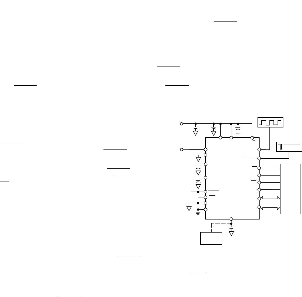
TYPICAL CONNECTION DIAGRAM
Figure 8 shows a typical connection diagram for the AD7859/
AD7859L. The AGND and the DGND pins are connected
together at the device for good noise suppression. The first
CONVST applied after power-up starts a self-calibration
sequence. This is explained in the calibration section of this data
sheet. Note that after power is applied to AV
DD
and DV
DD
and
the
CONVST signal is applied, the part requires (70 ms + 1/
sample rate) for the internal reference to settle and for the self-
calibration on power-up to be completed.
AV
DD
DV
DD
AIN(+)
AIN(–)
C
REF1
C
REF2
SLEEP
DB15
DB0
CONVST
AGND
DGND
CLKIN
REF
IN
/REF
OUT
AD7859/
AD7859L
ANALOG
SUPPLY
+3V TO +5V
0.1µF
0.1µF10µF
0.1µF
0.01µF
CONVERSION
START SIGNAL
0.1nF EXTERNAL REF
0.1µF INTERNAL REF
CAL
0V TO 2.5V
INPUT
4MHz/1.8MHz
OSCILLATOR
OPTIONAL
EXTERNAL
REFERENCE
CS
RD
WR
W/B
BUSY
DV
DD
µC/µP
AD780/
REF192
Figure 8. Typical Circuit
For applications where power consumption is a major concern,
the power-down options can be exercised by writing to the part
and using the
SLEEP pin. See the Power-Down section for more
details on low power applications.
CIRCUIT INFORMATION
The AD7859/AD7859L is a fast, 8-channel, 12-bit, single sup-
ply A/D converter. The part requires an external 4 MHz/1.8
MHz master clock (CLKIN), two C
REF
capacitors, a CONVST
signal to start conversion and power supply decoupling capaci-
tors. The part provides the user with track/hold, on-chip refer-
ence, calibration features, A/D converter and parallel interface
logic functions on a single chip. The A/D converter section of
the AD7859/AD7859L consists of a conventional successive-ap-
proximation converter based around a capacitor DAC. The
AD7859/AD7859L accepts an analog input range of 0 to +V
REF.
V
REF
can be tied to V
DD
. The reference input to the part con-
nected via a 150 k resistor to the internal 2.5 V reference and
to the on-chip buffer.
A major advantage of the AD7859/AD7859L is that a conver-
sion can be initiated in software, as well as by applying a signal
to the
CONVST pin. The part is available in a 44-pin PLCC or a
44-pin PQFP package, and this offers the user considerable
spacing saving advantages over alternative solutions. The
AD7859L version typically consumes only 5.5 mW making it
ideal for battery-powered applications.
CONVERTER DETAILS
The master clock for the part is applied to the CLKIN pin.
Conversion is initiated on the AD7859/AD7859L by pulsing the
CONVST input or by writing to the control register and setting
the CONVST bit to 1. On the rising edge of
CONVST (or at
the end of the control register write operation), the on-chip
track/hold goes from track to hold mode. The falling edge of the
CLKIN signal which follows the rising edge of
CONVST ini-
tiates the conversion, provided the rising edge of
CONVST (or
WR when converting via the control register) occurs typically at
least 10 ns before this CLKIN edge. The conversion takes 16.5
CLKIN periods from this CLKIN falling edge. If the 10 ns set-
up time is not met, the conversion takes 17.5 CLKIN periods.
The time required by the AD7859/AD7859L to acquire a signal
depends upon the source resistance connected to the AIN(+) in-
put. Please refer to the acquisition time section for more details.
When a conversion is completed, the BUSY output goes low,
and the result of the conversion can be read by accessing the
data through the data bus. To obtain optimum performance
from the part, read or write operations should not occur during
the conversion or less than 200 ns prior to the next
CONVST
rising edge. Reading/writing during conversion typically de-
grades the Signal-to-(Noise + Distortion) by less than 0.5 dBs.
The AD7859 can operate at throughput rates of over 200 kSPS
(up to 100 kSPS for the AD7859L).
With the AD7859L, 100 kSPS throughput can be obtained as
follows: the CLKIN and
CONVST signals are arranged to give
a conversion time of 16.5 CLKIN periods as described above

AD7859ASZ

Mfr. #:
Manufacturer:
Analog Devices Inc.
Description:
Analog to Digital Converters - ADC 3-5V SGL Supply 200kSPS 8-Ch 12-Bit
Lifecycle:
New from this manufacturer.
Delivery:
DHL FedEx Ups TNT EMS
Payment:
T/T Paypal Visa MoneyGram Western Union