AD7859/AD7859L
REV. A
–21–
CALIBRATION SECTION
Calibration Overview
The automatic calibration that is performed on power-up
ensures that the calibration options covered in this section are
not required in a significant number of applications. A calibra-
tion does not have to be initiated unless the operating condi-
tions change (CLKIN frequency, analog input mode, reference
voltage, temperature, and supply voltages). The AD7859/
AD7859L has a number of calibration features that may be
required in some applications, and there are a number of advan-
tages in performing these different types of calibration. First, the
internal errors in the ADC can be reduced significantly to give
superior dc performance; and second, system offset and gain er-
rors can be removed. This allows the user to remove reference
errors (whether it be internal or external reference) and to make
use of the full dynamic range of the AD7859/AD7859L by ad-
justing the analog input range of the part for a specific system.
There are two main calibration modes on the AD7859/AD7859L,
self-calibration and system calibration. There are various op-
tions in both self-calibration and system calibration as outlined
previously in Table IV. All the calibration functions are initi-
ated by writing to the control register and setting the STCAL
bit to 1.
The duration of each of the different types of calibration is given
in Table IX for the AD7859 with a 4 MHz master clock. These
calibration times are master clock dependent. Therefore the
calibration times for the AD7859L (CLKIN = 1.8 MHz) are
larger than those quoted in Table IX.
Table IX. Calibration Times (AD7859 with 4 MHz CLKIN)
Type of Self-Calibration or System Calibration Time
Full 31.25 ms
Gain + Offset 6.94 ms
Offset 3.47 ms
Gain 3.47 ms
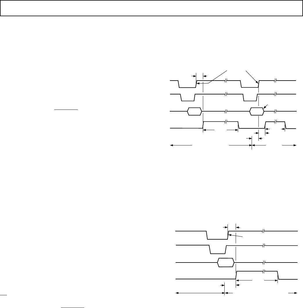
Calibration on Power-On
The calibration on power-on is initiated by the first CONVST
pulse after the AV
DD
and DV
DD
power on. From the CONVST
pulse the part internally sets a 32/72 ms (4 MHz/1.8 MHz
CLKIN) timeout. This time is large enough to ensure that the
internal reference has settled before the calibration is performed.
However, if an external reference is being used, this reference
must have stabilized before the automatic calibration is initiated.
This first
CONVST pulse also triggers the BUSY signal high,
and once the 32/72 ms has elapsed, the BUSY signal goes low.
At this point the next
CONVST pulse that is applied initiates
the automatic full self-calibration. This
CONVST pulse again
triggers the BUSY signal high, and after 32/72 ms (4 MHz/
1.8 MHz CLKIN), the calibration is completed and the BUSY
signal goes low. This timing arrangement is shown in Figure 28.
The times in Figure 28 assume a 4 MHz/1.8 MHz CLKIN signal.
AV
DD
= DV
DD
CONVST
BUSY
POWER-ON
32/72ms
32/72ms
TIMEOUT PERIOD AUTOMATIC
CALIBRATION
DURATION
CONVERSION IS INITIATED
ON THIS EDGE
Figure 28. Timing Arrangement for Autocalibration on
Power-On
The CONVST signal is gated with the BUSY internally so that
as soon as the timeout is initiated by the first
CONVST pulse all
subsequent
CONVST pulses are ignored until the BUSY signal
goes low, 32/72 ms later. The
CONVST pulse that follows after
the BUSY signal goes low initiates a full self-calibration. This
takes a further 32/72 ms. After calibration, the part is accurate
to the 12-bit level and the specifications quoted on the data
sheet apply; all subsequent
CONVST pulses initiate conver-
sions. There is no need to perform another calibration unless
the operating conditions change or unless a system calibration is
required.
This autocalibration at power-on is disabled if the user writes to
the control register before the autocalibration is initiated. If the
control register write operation occurs during the first 32/72 ms
timeout period, then the BUSY signal stays high for the 32/72
ms and the
CONVST pulse that follows the BUSY going low
does not initiate a full self-calibration. It initiates a conversion
and all subsequent
CONVST pulses initiate conversions as well.
If the control register write operation occurs when the automatic
full self-calibration is in progress, then the calibration is not be
aborted; the BUSY signal remains high until the automatic full
self-calibration is complete.
Self-Calibration Description
There are four different calibration options within the self-
calibration mode. There is a full self-calibration where the
DAC, internal offset, and internal gain errors are removed.
There is the (Gain + Offset) self-calibration which removes the
internal gain error and then the internal offset errors. The inter-
nal DAC is not calibrated here. Finally, there are the self-offset
and self-gain calibrations which remove the internal offset errors
and the internal gain errors respectively.
The internal capacitor DAC is calibrated by trimming each of
the capacitors in the DAC. It is the ratio of these capacitors to
each other that is critical, and so the calibration algorithm en-
sures that this ratio is at a specific value by the end of the cali-
bration routine. For the offset and gain there are two separate
capacitors, one of which is trimmed during offset calibration
and one of which is trimmed during gain calibration.
In Bipolar Mode the midscale error is adjusted by an offset cali-
bration and the positive full-scale error is adjusted by the gain
calibration. In Unipolar Mode the zero-scale error is adjusted
by the offset calibration and the positive full-scale error is ad-
justed by the gain calibration.
AD7859/AD7859L
REV. A
–22–
Self-Calibration Timing
Figure 29 shows the timing for a software full self-calibration.
Here the BUSY line stays high for the full length of the self-
calibration. A self-calibration is initiated by writing to the
control register and setting the STCAL bit to 1. The BUSY line
goes high at the end of the write to the control register, and
BUSY goes low when the full self-calibration is complete after a
time t
CAL
as show in Figure 29.
t
19
DATA LATCHED INTO
CONTROL REGISTER
HI-Z HI-Z
DATA
VALID
CS
WR
DATA
BUSY
t
CAL
Figure 29. Timing Diagram for Full Self-Calibration
For the self-(gain + offset), self-offset and self-gain calibrations,
the BUSY line is triggered high at the end of the write to the
control register and stays high for the full duration of the self-
calibration. The length of time for which BUSY is high depends
on the type of self-calibration that is initiated. Typical values are
given in Table IX. The timing diagram for the other self-calibration
options is similar to that outlined in Figure 29.
System Calibration Description
System calibration allows the user to remove system errors ex-
ternal to the AD7859/AD7859L, as well as remove the errors of
the AD7859/AD7859L itself. The maximum calibration range
for the system offset errors is ±5% of V
REF
and for the system
gain errors, it is ±2.5% of V
REF
. If the system offset or system
gain errors are outside these ranges, the system calibration algo-
rithm reduces the errors as much as the trim range allows.
Figures 30 through 32 illustrate why a specific type of system
calibration might be used. Figure 30 shows a system offset cali-
bration (assuming a positive offset) where the analog input
range has been shifted upwards by the system offset after the
system offset calibration is completed. A negative offset may
also be removed by a system offset calibration.
MAX SYSTEM FULL SCALE
IS ±2.5% FROM V
REF
MAX SYSTEM OFFSET
IS ±5% OF V
REF
ANALOG
INPUT
RANGE
V
REF
+ SYS OFFSET
V
REF
– 1LSB
SYSTEM OFFSET
CALIBRATION
SYS OFFSET
AGND
ANALOG
INPUT
RANGE
V
REF
– 1LSB
SYS OFFSET
AGND
MAX SYSTEM OFFSET
IS ±5% OF V
REF
Figure 30. System Offset Calibration
Figure 31 shows a system gain calibration (assuming a system
full scale greater than the reference voltage) where the analog
input range has been increased after the system gain calibration
is completed. A system full-scale voltage less than the reference
voltage may also be accounted for a by a system gain calibration.
ANALOG
INPUT
RANGE
MAX SYSTEM FULL SCALE
IS ±2.5% FROM V
REF
SYSTEM GAIN
CALIBRATION
ANALOG
INPUT
RANGE
V
REF
– 1LSB
AGND
SYS FULL S.
MAX SYSTEM FULL SCALE
IS ±2.5% FROM V
REF
V
REF
– 1LSB
SYS FULL S.
AGND
Figure 31. System Gain Calibration
Finally in Figure 32 both the system offset error and gain error
are removed by the system offset followed by a system gain cali-
bration. First the analog input range is shifted upwards by the
positive system offset and then the analog input range is adjusted at
the top end to account for the system full scale.
MAX SYSTEM FULL SCALE
IS ±2.5% FROM V
REF
ANALOG
INPUT
RANGE
V
REF
+ SYS OFFSET
SYS OFFSET
AGND
ANALOG
INPUT
RANGE
V
REF
– 1LSB
SYS OFFSET
AGND
MAX SYSTEM OFFSET
IS ±5% OF V
REF
MAX SYSTEM OFFSET
IS ±5% OF V
REF
SYSTEM GAIN
CALIBRATION
SYSTEM OFFSET
CALIBRATION
FOLLOWED BY
V
REF
– 1LSB
SYS F.S.
SYS F.S.
MAX SYSTEM FULL SCALE
IS ±2.5% FROM V
REF
Figure 32. System (Gain + Offset) Calibration
AD7859/AD7859L
REV. A
–23–
System Gain and Offset Interaction
The architecture of the AD7859/AD7859L leads to an interac-
tion between the system offset and gain errors when a system
calibration is performed. Therefore, it is recommended to per-
form the cycle of a system offset calibration followed by a sys-
tem gain calibration twice. When a system offset calibration is
performed, the system offset error is reduced to zero. If this is
followed by a system gain calibration, then the system gain error
is now zero, but the system offset error is no longer zero. A sec-
ond sequence of system offset error calibration followed by a
system gain calibration is necessary to reduce system offset error
to below the 12-bit level. The advantage of doing separate
system offset and system gain calibrations is that the user has
more control over when the analog inputs need to be at the
required levels, and the
CONVST signal does not have to be
used.
Alternatively, a system (gain + offset) calibration can be per-
formed. At the end of one system (gain + offset) calibration, the
system offset error is zero, while the system gain error is reduced
from its initial value. Three system (gain + offset) calibrations
are required to reduce the system gain error to below the 12-bit
error level. There is never any need to perform more than three
system (gain + offset) calibrations.
In bipolar mode the midscale error is adjusted for an offset cali-
bration and the positive full-scale error is adjusted for the gain
calibration; in unipolar mode the zero-scale error is adjusted for
an offset calibration and the positive full-scale error is adjusted
for a gain calibration.
System Calibration Timing
The timing diagram in Figure 33 is for a software full system
calibration. It may be easier in some applications to perform
separate gain and offset calibrations so that the CONVST bit in
the control register does not have to be programmed in the
middle of the system calibration sequence. Once the write to the
control register setting the bits for a full system calibration is
completed, calibration of the internal DAC is initiated and the
BUSY line goes high. The full-scale system voltage should be
applied to the analog input pins, AIN(+) and AIN(–) at the start
of calibration. The BUSY line goes low once the DAC and sys-
tem gain calibration are complete. Next the system offset volt-
age should be applied across the AIN(+) and AIN(–) pins for a
minimum setup time (t
SETUP
) of 100 ns before the rising edge of
CS. This second write to the control register sets the CONVST
bit to 1 and at the end of this write operation the BUSY signal is
triggered high (note that a
CONVST pulse can be applied in-
stead of this second write to the control register). The BUSY
signal is low after a time t
CAL2
when the system offset calibration
section is complete. The full system calibration is now complete.
The timing for a system (gain + offset) calibration is very similar
to that of Figure 33, the only difference being that the time
t
CAL1
is replaced by a shorter time of the order of t
CAL2
as the in-
ternal DAC is not calibrated. The BUSY signal signifies when
the gain calibration is finished and when the part is ready for the
offset calibration.
t
19
DATA LATCHED INTO
CONTROL REGISTER
HI-Z
HI-Z
HI-Z
t
19
t
SETUP
DATA
VALID
t
CAL1
t
CAL2
V
OFFSET
CONVST BIT SET TO 1 IN
CONTROL REGISTER
CS
WR
DATA
BUSY
AIN
DATA
VALID
V
SYSTEM FULL SCALE
Figure 33. Timing Diagram for Full System Calibration
The timing diagram for a system offset or system gain calibra-
tion is shown in Figure 34. Here again a write to the control reg-
ister initiates the calibration sequence. At the end of the control
register write operation the BUSY line goes high and it stays
high until the calibration sequence is finished. The analog input
should be set at the correct level for a minimum setup time
(t
SETUP
) of 100 ns before the CS rising edge and stay at the cor-
rect level until the BUSY signal goes low.
t
19
HI-Z
HI-Z
DATA LATCHED INTO
CONTROL REGISTER
t
SETUP
BUSY
AIN
CS
WR
DATA
DATA
VALID
t
CAL2
V
SYSTEM FULL SCALE
OR V
OFFSET
Figure 34. Timing Diagram for System Gain or
System Offset Calibration

AD7859ASZ

Mfr. #:
Manufacturer:
Analog Devices Inc.
Description:
Analog to Digital Converters - ADC 3-5V SGL Supply 200kSPS 8-Ch 12-Bit
Lifecycle:
New from this manufacturer.
Delivery:
DHL FedEx Ups TNT EMS
Payment:
T/T Paypal Visa MoneyGram Western Union