AD7859/AD7859L
REV. A
–26–
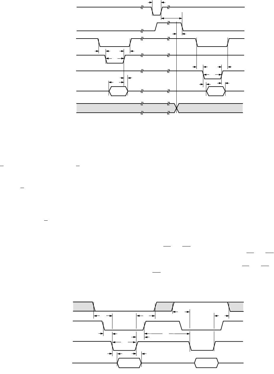
The parallel interface on the AD7859/AD7859L is fast enough
to interface to the TMS32020 with no extra wait states. If high
speed glue logic such as 74AS devices are used to drive the
WR
and
RD lines when interfacing to the TMS320C25, then again
no wait states are necessary. However, if slower logic is used,
data accesses may be slowed sufficiently when reading from and
writing to the part to require the insertion of one wait state. In
such a case, this wait state can be generated using the single OR
gate to combine the
CS and MSC signals to drive the READY
line of the TMS320C25, as shown in Figure 39. Extra wait
states will be necessary when using the TMS320C5x at their
fastest clock speeds. Wait states can be programmed via the
IOWSR and CWSR registers (please see TMS320C5x User
Guide for details).
Data is read from the ADC using the following instruction:
IN D,ADC
where D is the memory location where the data is to be stored
and ADC is the I/O address of the AD7859/AD7859L.
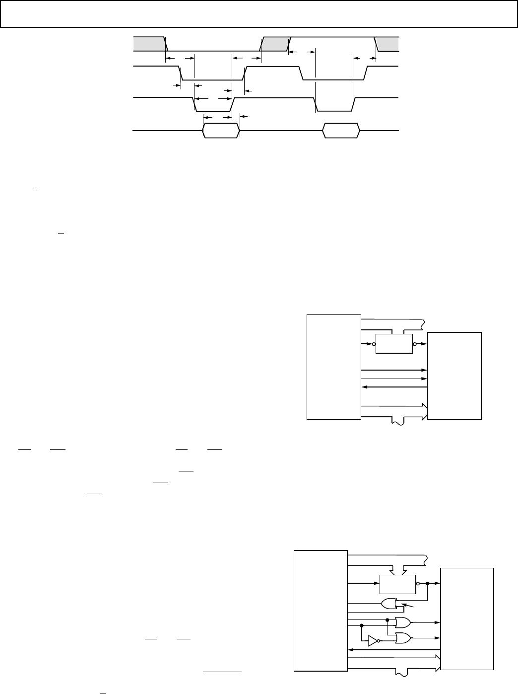
AD7859/AD7859L to TMS320C30
Figure 40 shows a parallel interface between the AD7859/
AD7859L and the TMS320C3x family of DSPs. The AD7859/
AD7859L is interfaced to the Expansion Bus of the TMS320C3x.
A single wait state is required in this interface. This can be pro-
grammed using the WTCNT bits of the Expansion Bus Control
register (see TMS320C3x Users Guide for details). Data from
the AD7859/AD7859L can be read using the following instruction:
LDI *ARn,Rx
where ARn is an auxiliary register containing the lower 16 bits
of the address of the AD7859/AD7859L in the TMS320C3x
memory space and Rx is the register into which the ADC data is
loaded.
TMS320C30*
CS
DB15–DB0
AD7859/
AD7859L*
*ADDITIONAL PINS OMITTED FOR CLARITY
XD23–XD0
ADDR
DECODE
EXPANSION DATA BUS
WR
RD
EXPANSION ADDRESS BUS
IOSTRB
INTx
XA12–XA0
XR/W
BUSY
Figure 40. AD7859/AD7859L to TMS320C30 Parallel Interface
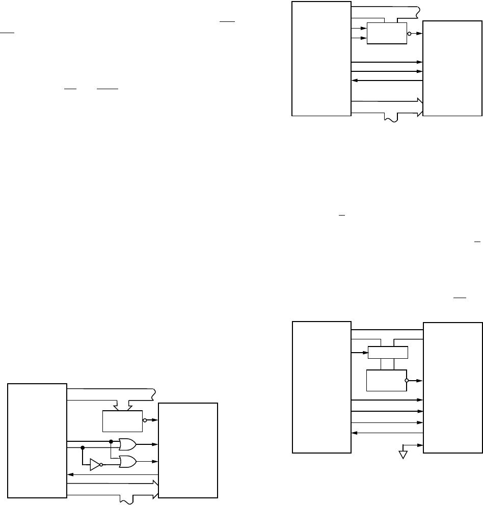
AD7859/AD7859L to DSP5600x
Figure 41 shows a parallel interface between the AD7859/
AD7859L and the DSP5600x series of DSPs. The AD7859/
AD7859L should be mapped into the top 64 locations of Y data
memory. If extra wait states are needed in this interface, they
can be programmed using the Port A Bus Control Register
(please see DSP5600x Users Manual for details). Data can be
read from the AD7859/AD7859L using the following instruction:
MOVEO Y:ADC,X0
where ADC is the address in the DSP5600x address space
which the AD7859/AD7859L has been mapped to.
DSP56000/
DSP56002*
CS
DB15–DB0
AD7859/
AD7859L*
*ADDITIONAL PINS OMITTED FOR CLARITY
D23–D0
ADDR
DECODE
DS
DATA BUS
WR
RD
ADDRESS BUS
WR
RD
IRQ
A15–A0
X/Y
BUSY
Figure 41. AD7859/AD7859L to DSP5600x Parallel Interface
Interfacing the AD7859/AD7859L to an 8-Bit Data Bus
AD7859/AD7859L to 8051
This mode of operation allows the AD7859/AD7859L to be in-
terfaced directly to microcontrollors with an 8-bit data bus. The
AD7859/AD7859L is placed in byte mode by placing a logic
low signal on the W/
B pin.
Figure 42 shows a parallel interface between the AD7859/
AD7859L and the 8051 microcontroller. Here the W/
B pin is
tied logic low and the DB8/HBEN pin connected to line 1 of
Port 2. Port 0 serves as a multiplexed address/data bus to the
AD7859/AD7859L. Alternatively if the 8051 is not using exter-
nal memory or other memory mapped peripheral devices, line 2
of Port 2 (or any other line) could be used as the
CS signal.
8051*
ADDR
DECODE
CS
DB7–DB0
AD7859/
AD7859L*
*ADDITIONAL PINS OMITTED FOR CLARITY
WR
RD
WR
RD
INT0
P0
BUSY
LATCH
ALE
P2.1 DB8/HBEN
W/B
DGND
Figure 42. AD7859/AD7859L to 8051 Parallel Interface
APPLICATION HINTS
Grounding and Layout
The analog and digital supplies of the AD7859/AD7859L are
independent and separately pinned out to minimize coupling
between the analog and digital sections of the device. The part
has very good immunity to noise on the power supplies as can
be seen by the PSRR versus Frequency graph. However, care
should still be taken with regard to grounding and layout.
The printed circuit board on which the AD7859/AD7859L is
mounted should be designed such that the analog and digital
sections are separated and confined to certain areas of the
board. This facilitates the use of ground planes that can be eas-
ily separated. A minimum etch technique is generally best for
ground planes as it gives the best shielding. Digital and analog
ground planes should only be joined in one place. If the
AD7859/AD7859L is the only device requiring an AGND to