BELASIGNA 250
http://onsemi.com
20
Table 9. INTERRUPT DESCRIPTIONS
Interrupt Description
WOLA_DONE WOLA function done
IO_BLOCK_FULL IOP interrupt
GP_TIMER General−purpose timer interrupt
WATCHDOG_TIMER Watchdog timer interrupt
SPI_INTERFACE SPI interface interrupt
IR IR remote interrupt
EXT3_RX EXT3 register receive interrupt
EXT3_TX EXT3 register transmit interrupt
GPIO User configurable GPIO interrupt
TWSS_INTERFACE Two−wire synchronous serial interface interrupt
UART_RX General−purpose UART receive interrupt
UART_TX General−purpose UART transmit interrupt
PCM PCM interface interrupt
Analog Blocks
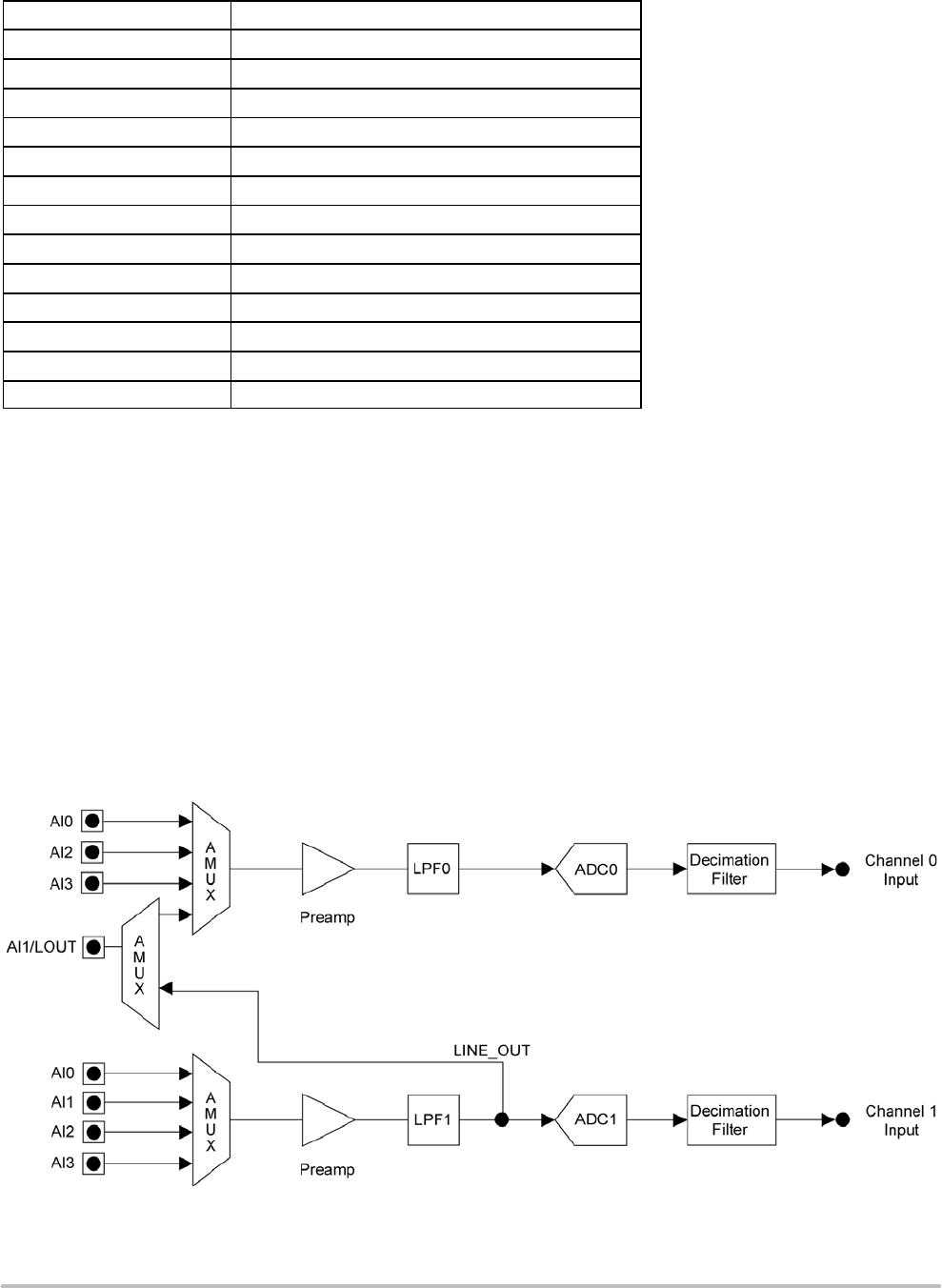
Input Stage
The analog audio input stage is comprised of two
individual channels. For each channel, the selected one out
of the four possible inputs is routed to the input of the
programmable preamplifier that can be configured for
bypass or gain values of 12 to 30 dB (3 dB steps).
The analog signal is filtered to remove frequencies above
20 kHz before it is passed into the high−fidelity 16−bit
oversampling SD A/D converter. Subsequently, any
necessary sample rate decimation is performed to
downsample the signal to the desired sampling rate. During
decimation the level of the signal can be adjusted digitally
for optimal gain matching between the two input channels.
Any undesired DC component can be removed by a
configurable DC−removal filter that is part of the
decimation circuitry. The DC removal filter can be
configured for bypass or cut−off frequencies at 5, 10 and
20 Hz.
A built−in feature allows a sampling delay to be
configured between channel zero and channel one (or vice
versa). This is useful in beam−forming applications.
Note: Both preamplifiers can be daisy−chained to increase
the potential gain, but the signal has to be routed externally
to the chip.
For power consumption savings either of the input
channels can be disabled via software. A different input
must be selected for each channel. The input stage is shown
in Figure 7.
Figure 7. Input Stage

