BELASIGNA 250
http://onsemi.com
5
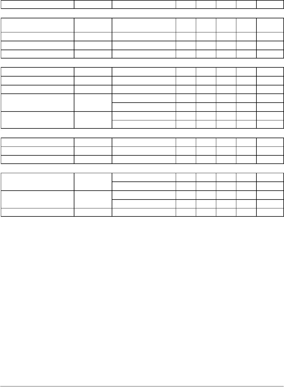
Table 2. ELECTRICAL SPECIFICATIONS (continued)
Description ScreenedUnitsMaxTypMinConditionsSymbol
ANALOG OUTPUT STAGE
Attenuator gain tolerance
ATG Input is –6 dB re: full scale @
1 kHz (all preamplifier gains)
−1 − 1 dB √
Output impedance R
OUT
Attenuator settings:
0 dB
12 dB
15 dB
18 dB
21 dB
24 dB
27 dB
30 dB
1
9
7
4
3
2
1
1
2
13
10
8
6
4
3
2
5
17
14
12
9
7
6
5
kW
√
Output noise OUT
N
0 dB attenuation − 33 40
mV
Output dynamic range OUT
DR
Unweighted, 100 Hz to
8 kHz BW, mono
85 87 − dB
Output THD+N OUT
THDN
Unweighted, 100 Hz to
22 kHz BW, mono
− −70 −67 dB
ANTI−ALIASING FILTERS (Input and Output)
Preamplifier filter cut−off frequency
Preamp not bypassed − 25 − kHz
Digital anti−aliasing filter cut−off
frequency
− f
s
/2 −
Analog output cut−off frequency
25 kHz 15 25 35 kHz
12 kHz (only output filter) 9 12 15 kHz
Passband flatness −1 − 1 dB
Stopband attenuation 60 kHz (12 kHz cut−off) − 60 − dB
LOW−SPEED A/D
Input voltage
Peak input voltage 0 − 2.0 V √
INL From GND to 2*VREG − − 10 LSB
DNL From GND to 2*VREG − − 2 LSB
Maximum variation over
temperature (0_C to 50_C)
− − 5 LSB
Sampling frequency All channels sequentially − 12.8 − kHz
Channel sampling frequency 8 channels − 1.6 − kHz
DIGITAL PADS
Voltage level for high input
V
IH
VDDC
* 0.8
− VDDC
+ 0.5
(Note 6)
V
Voltage level for low input V
IL
−0.3 − VDDC
* 0.2
V
Input capacitance for digital pads C
IN
− 2 − pF
Pull−up resistance for digital input
pads
R
UP_IN
− 260 −
kW
√
Pull−down resistance to VDDC fo
digital input pads
R
DOWN_IN
VDDC = 1.0 V − 430 −
kW
VDDC = 1.25 V − 260 −
kW
√
VDDC = 2.0 V − 140 −
kW
3. Audio performance will be degraded below 1.05 V.
4. Measured with a = 12 dB input signal.
5. Input stage delay is inversely proportional to sampling frequency.
6. Max voltage should be limited to 2.2 V peak regardless of VDDC. Protection diodes will be enabled above this voltage.