Si4734/35-C40
14 Rev. 1.0
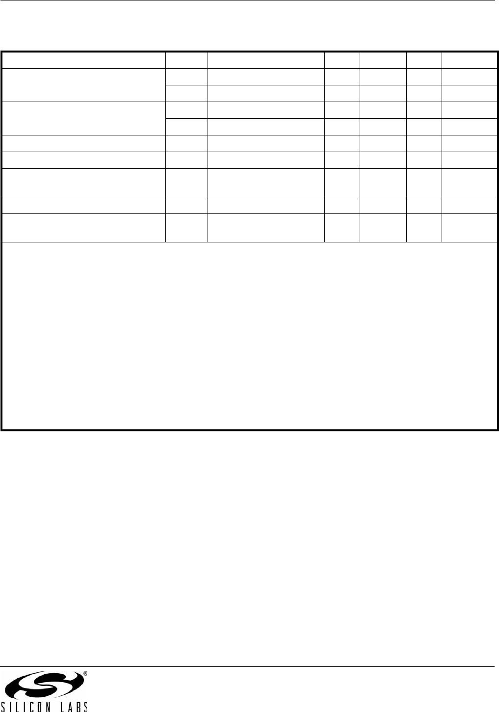
Table 10. 64–75.9 MHz Input Frequency FM Receiver Characteristics
1,2,6
(V
DD
= 2.7 to 5.5 V, V
IO
= 1.85 to 3.6 V, T
A
= –20 to 85 °C)
Parameter Symbol Test Condition Min Typ Max Unit
Input Frequency f
RF
64 — 75.9 MHz
Sensitivity with Headphone
Network
3,4,5
(S+N)/N = 26 dB — 4.0 — µV EMF
LNA Input Resistance
7
345k
LNA Input Capacitance
7
456pF
Input IP3
8
100 105 — dBµV EMF
AM Suppression
3,4,7
m = 0.3 40 50 — dB
Adjacent Channel Selectivity
±200 kHz — 50 — dB
Alternate Channel Selectivity
±400 kHz — 70 — dB
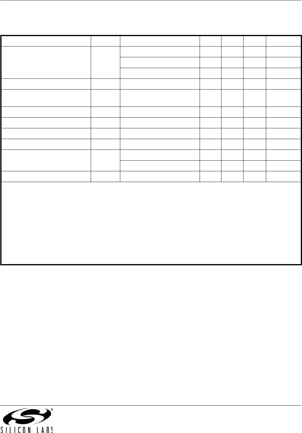
Audio Output Voltage
3,4,7
72 80 90 mV
RMS
Audio Output L/R Imbalance
3,7,9
—— 1 dB
Audio Frequency Response Low
–3 dB — — 30 Hz
Audio Frequency Response High
–3 dB 15 — — kHz
Audio Mono S/N
3,4,5,7,10
55 63 — dB
Audio THD
3,7,9
—0.10.5 %
De-emphasis Time Constant FM_DEEMPHASIS = 2 70 75 80 µs
FM_DEEMPHASIS = 1 45 50 54 µs
Audio Output Load Resistance
10
R
L
Single-ended 10 — — k
Audio Output Load Capacitance
10
C
L
Single-ended — — 50 pF
Seek/Tune Time RCLK tolerance
=100ppm
— — 60 ms/channel
Powerup Time From powerdown — — 110 ms
RSSI Offset
11
Input levels of 8 and
60 dBµV EMF
–3 — 3 dB
Notes:
1. Additional testing information is available in “AN388: Si470x/1x/2x/3x/4x Evaluation Board Test Procedure.”
Volume = maximum for all tests. Tested at RF = 98.1 MHz.
2. To ensure proper operation and receiver performance, follow the guidelines in “AN383: Si47xx Antenna, Schematic,
Layout, and Design Guidelines.” Silicon Laboratories will evaluate schematics and layouts for qualified customers.
3. F
MOD
=1kHz, 75µs de-emphasis, MONO = enabled, and L = R unless noted otherwise.
4. f = 22.5 kHz.
5. B
AF
= 300 Hz to 15 kHz, A-weighted.
6. Guaranteed by characterization.
7. V
EMF
=1 mV.
8. |f
2
– f
1
| > 2 MHz, f
0
=2xf
1
– f
2
. AGC is disabled.
9. f = 75 kHz.
10. At L
OUT
and R
OUT
pins.
11. At temperature (25 °C).