Si4734/35-C40
4 Rev. 1.0
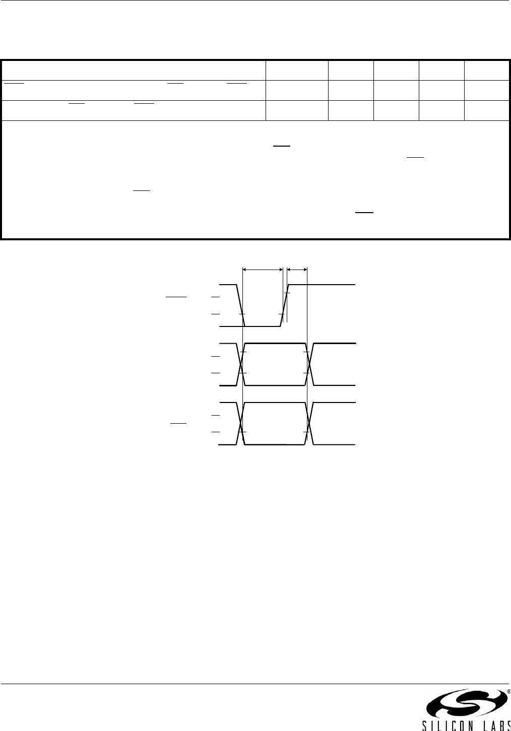
1. Electrical Specifications
Table 1. Recommended Operating Conditions
1
Parameter Symbol Test Condition Min Typ Max Unit
Supply Voltage
2
V
DD
2.7 — 5.5 V
Interface Supply Voltage V
IO
1.85 — 3.6 V
Power Supply Powerup Rise Time V
DDRISE
10 — — µs
Interface Power Supply Powerup Rise Time V
IORISE
10 — — µs
Ambient Temperature T
A
–20 25 85 C
Note:
1. All minimum and maximum specifications apply across the recommended operating conditions. Typical values apply at
V
DD
= 3.3 V and 25 C unless otherwise stated.
2. SSOP devices operate down to V
DD
= 2 V at 25 °C.
Table 2. Absolute Maximum Ratings
1,2
Parameter Symbol Value Unit
Supply Voltage V
DD
–0.5 to 5.8 V
Interface Supply Voltage V
IO
–0.5 to 3.9 V
Input Current
3
I
IN
10 mA
Input Voltage
3
V
IN
–0.3 to (V
IO
+ 0.3) V
Operating Temperature T
OP
–40 to 95 C
Storage Temperature T
STG
–55 to 150 C
RF Input Level
4
0.4 V
PK
Notes:
1. Permanent device damage may occur if the above Absolute Maximum Ratings are exceeded. Functional operation
should be restricted to the conditions as specified in the operational sections of this data sheet. Exposure beyond
recommended operating conditions for extended periods may affect device reliability.
2. The Si4734/35 devices are high-performance RF integrated circuits with certain pins having an ESD rating of < 2 kV
HBM. Handling and assembly of these devices should only be done at ESD-protected workstations.
3. For input pins SCLK, SEN, SDIO, RST, RCLK, DCLK, DFS, GPO1, GPO2, and GPO3.
4. At RF input pins, FMI and AMI.