Si4734/35-C40
Rev. 1.0 7
Table 5. 2-Wire Control Interface Characteristics
1,2,3
(V
DD
= 2.7 to 5.5 V, V
IO
= 1.85 to 3.6 V, T
A
= –20 to 85 °C)
Parameter Symbol Test Condition Min Typ Max Unit
SCLK Frequency f
SCL
0—400kHz
SCLK Low Time t
LOW
1.3 µs
SCLK High Time t
HIGH
0.6 µs
SCLK Input to SDIO
Setup
(START)
t
SU:STA
0.6 µs
SCLK Input to SDIO
Hold
(START)
t
HD:STA
0.6 µs
SDIO Input to SCLK
Setup t
SU:DAT
100 ns
SDIO Input to SCLK
Hold
4,5
t
HD:DAT
0—900ns
SCLK input to SDIO
Setup
(STOP)
t
SU:STO
0.6 µs
STOP to START Time t
BUF
1.3 µs
SDIO Output Fall Time t
f:OUT
—250ns
SDIO Input, SCLK Rise/Fall Time t
f:IN
t
r:IN
—300ns
SCLK, SDIO Capacitive Loading C
b
——50pF
Input Filter Pulse Suppression t
SP
50 ns
Notes:
1. When V
IO
= 0 V, SCLK and SDIO are low impedance.
2. When selecting 2-wire mode, the user must ensure that a 2-wire start condition (falling edge of SDIO while SCLK is
high) does not occur within 300 ns before the rising edge of RST.
3. When selecting 2-wire mode, the user must ensure that SCLK is high during the rising edge of RST
, and stays high
until after the first start condition.
4. The Si4734/35 delays SDIO by a minimum of 300 ns from the V
IH
threshold of SCLK to comply with the minimum
t
HD:DAT
specification.
5. The maximum t
HD:DAT
has only to be met when f
SCL
= 400 kHz. At frequencies below 400 KHz, t
HD:DAT
may be
violated as long as all other timing parameters are met.
20 0.1
C
b
1pF
-----------
+
20 0.1
C
b
1pF
-----------
+
Si4734/35-C40
8 Rev. 1.0
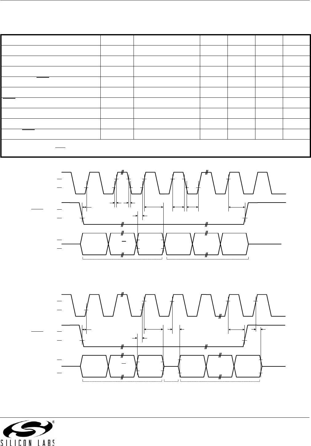
Figure 2. 2-Wire Control Interface Read and Write Timing Parameters
Figure 3. 2-Wire Control Interface Read and Write Timing Diagram
SCLK
70%
30%
SDIO
70%
30%
START
STARTSTOP
t
f:IN
t
r:IN
t
LOW
t
HIGH
t
HD:STA
t
SU:STA
t
SU:STO
t
SP
t
BUF
t
SU:DAT
t
r:IN
t
HD:DAT
t
f:IN,
t
f:OUT
SCLK
SDIO
START STOPADDRESS + R/W ACK DATA ACK DATA ACK
A6-A0,
R/W
D7-D0 D7-D0
Si4734/35-C40
Rev. 1.0 9
Figure 4. 3-Wire Control Interface Write Timing Parameters
Figure 5. 3-Wire Control Interface Read Timing Parameters
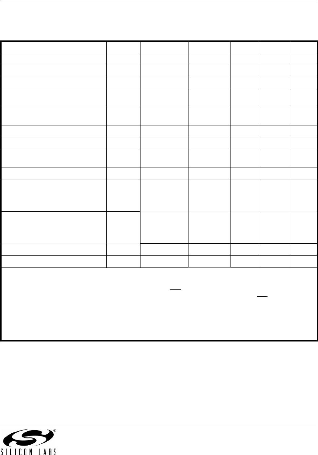
Table 6. 3-Wire Control Interface Characteristics
(V
DD
= 2.7 to 5.5 V, V
IO
= 1.85 to 3.6 V, T
A
= –20 to 85 °C)
Parameter Symbol Test Condition Min Typ Max Unit
SCLK Frequency f
CLK
0—2.5MHz
SCLK High Time t
HIGH
25 ns
SCLK Low Time t
LOW
25 ns
SDIO Input, SEN
to SCLKSetup t
S
20 ns
SDIO Input to SCLKHold t
HSDIO
10 ns
SEN
Input to SCLKHold t
HSEN
10 ns
SCLKto SDIO Output Valid t
CDV
Read 2 25 ns
SCLKto SDIO Output High Z t
CDZ
Read 2 25 ns
SCLK, SEN
, SDIO, Rise/Fall time t
R
, t
F
10 ns
Note: When selecting 3-wire mode, the user must ensure that a rising edge of SCLK does not occur within 300 ns before the
rising edge of RST
.
SCLK
70%
30%
SEN
70%
30%
SDIO
A7 A0
70%
30%
t
S
t
S
t
HSDIO
t
HSEN
A6-A5,
R/W,
A4-A1
Address In Data In
D15 D14-D1 D0
t
HIGH
t
LOW
t
R
t
F
½ Cycle Bus
Turnaround
SCLK
70%
30%
SEN
70%
30%
SDIO
70%
30%
t
HSDIO
t
CDV
t
CDZ
Address In Data Out
A7 A0
A6-A5,
R/W,
A4-A1
D15 D14-D1 D0
t
S
t
S
t
HSEN

SI4734-C40-GM

Mfr. #:
Manufacturer:
Silicon Labs
Description:
RF Receiver Si4734 rev C Broadcast AM/FM/SW/LW Radio Receiver 3x3x0.55 20-pin QFN, lead free
Lifecycle:
New from this manufacturer.
Delivery:
DHL FedEx Ups TNT EMS
Payment:
T/T Paypal Visa MoneyGram Western Union