Si4734/35-C40
Rev. 1.0 31
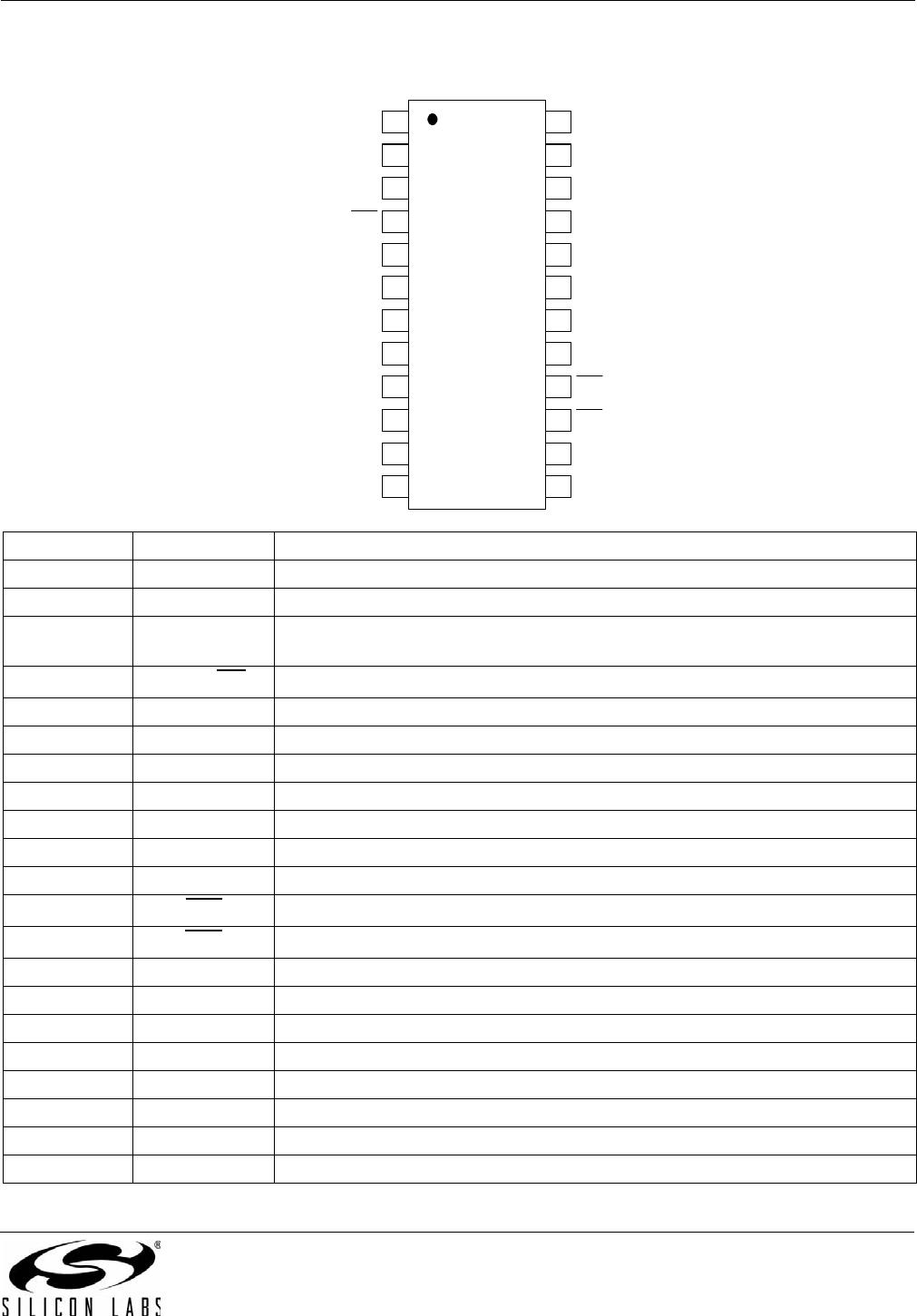
8. Pin Descriptions: Si4734/35-GU
Pin Number(s) Name Description
1 DOUT Digital output data in digital output mode.
2 DFS Digital frame synchronization input in digital output mode.
3 GPO3/DCLK General purpose output, crystal oscillator, or digital bit synchronous clock input
in digital output mode.
4 GPO2/INT
General purpose output or interrupt pin.
5 GPO1 General purpose output.
6,7 NC No connect. Leave floating.
8 FMI FM RF inputs. FMI should be connected to the antenna trace.
9 RFGND RF ground. Connect to ground plane on PCB.
10,11 NC Unused. Tie these pins to GND.
12 AMI AM/SW/LW RF input.
13,14 GND Ground. Connect to ground plane on PCB.
15 RST
Device reset (active low) input.
16 SEN
Serial enable input (active low).
17 SCLK Serial clock input.
18 SDIO Serial data input/output.
19 RCLK External reference oscillator input.
20 V
IO
I/O supply voltage.
21 V
DD
Supply voltage. May be connected directly to battery.
22 DBYP Dedicated bypass for V
DD
and V
IO
.
23 ROUT Right audio line output in analog output mode.
24 LOUT Left audio line output in analog output mode.
LOUT
ROUT
DBYP
VIO
GPO2/INT
GPO3/DCLK
DOUT
DFS
1
2
3
4
5
6
7
8
9
10
11
12
GPO1
VDD
SDIO
NC
NC
RCLK
SEN
FMI
RFGND
SCLK
GND
NC
NC
RST
GND
AMI
24
23
22
21
20
19
18
17
16
15
14
13
Si4734/35-C40
32 Rev. 1.0
9. Ordering Guide
Part Number* Description Package
Type
Operating
Temperature/Voltage
Si4734-C40-GM AM/FM/SW/LW Broadcast Radio Receiver QFN
Pb-free
–20 to 85 °C
2.7 to 5.5 V
Si4734-C40-GU AM/FM/SW/LW Broadcast Radio Receiver SSOP
Pb-free
–20 to 85 °C
2.0 to 5.5 V
Si4735-C40-GM AM/FM/SW/LW Broadcast Radio Receiver
with RDS/RBDS
QFN
Pb-free
–20 to 85 °C
2.7 to 5.5 V
Si4735-C40-GU AM/FM/SW/LW Broadcast Radio Receiver
with RDS/RBDS
SSOP
Pb-free
–20 to 85 °C
2.0 to 5.5 V
*Note: Add an “(R)” at the end of the device part number to denote tape and reel option; 2500 quantity per reel. SSOP
devices operate down to V
DD
= 2 V at 25 °C.
Si4734/35-C40
Rev. 1.0 33
10. Package Markings (Top Marks)
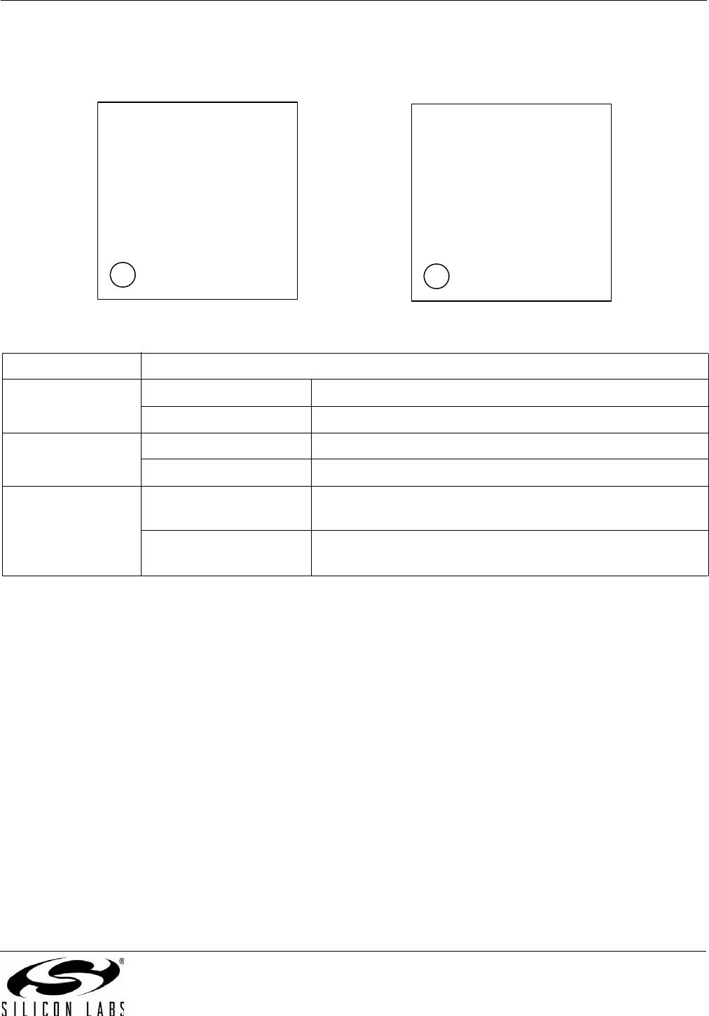
10.1. Si4734/35 Top Mark (QFN)
10.2. Top Mark Explanation (QFN)
Mark Method: YAG Laser
Line 1 Marking: Part Number 34 = Si4734, 35 = Si4735.
Firmware Revision 40 = Firmware Revision 4.0.
Line 2 Marking: Die Revision C = Revision C Die.
TTT = Internal Code Internal tracking code.
Line 3 Marking: Circle = 0.5 mm Diameter
(Bottom-Left Justified)
Pin 1 Identifier.
Y = Year
WW = Workweek
Assigned by the Assembly House. Corresponds to the last
significant digit of the year and work week of the mold date.
3440
CTTT
YWW
3540
CTTT
YWW

SI4734-C40-GM

Mfr. #:
Manufacturer:
Silicon Labs
Description:
RF Receiver Si4734 rev C Broadcast AM/FM/SW/LW Radio Receiver 3x3x0.55 20-pin QFN, lead free
Lifecycle:
New from this manufacturer.
Delivery:
DHL FedEx Ups TNT EMS
Payment:
T/T Paypal Visa MoneyGram Western Union