Si8220/21
Rev. 1.2 19
6.5. Parametric Differences between Si8220/21 and
HCPL-0302 and HCPL-3120 Opto Drivers
The Si8220/21 is designed to directly replace HCPL-3120 and similar opto drivers. Parametric differences are
summarized in Table 10 below.
6.5.1. Supply Voltage and UVLO
The supply voltage of the Si8220/21 is limited to 24 V, and the UVLO voltage thresholds are scaled accordingly.
Opto replacement applications should limit their supply voltages to 24 V or less.
6.5.2. Input Diode Differences
The Si8220/21 input circuit requires less current and has twice the off-state noise margin compared to opto drivers.
However, high CMR opto driver designs that overdrive the LED (see Figure 15) may require increasing the value of
R1 to limit input current to 20 mA max. In addition, there is no benefit in driving the Si8220/21 input diode into
reverse bias when in the off state. Consequently, opto driver circuits using this technique should either leave the
negative bias circuitry unpopulated or modify the circuitry (e.g. add a clamp diode) to ensure that the anode pin of
the Si8220/21 is no more than –0.8 V with respect to the cathode when reverse-biased.
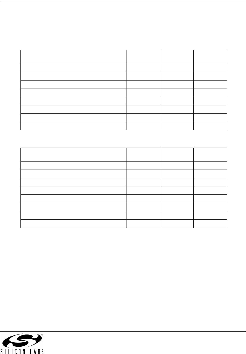
Table 10. Parametric Differences of Si8220 vs. HCPL-3120
Parameter Si8220 HCPL-3120 Units
Max supply voltage 24 30 V
ON state forward input current 5 to 20 7 to 16 mA
OFF state input voltage –0.6 to +1.6 –0.3 to +0.8 V
Max reverse input voltage 0.5 –5 V
UVLO threshold (rising) 5.8 to 13.8 11.0 to 13.5 V
UVLO threshold (falling) 5.5 to 12.8 9.7 to 12.0 V
UVLO hysteresis 0.28 to 1 1.6 V
Rise/fall time into 10 in series with 10 nF 20 100 ns
Table 11. Parametric Differences of Si8221 vs. HCPL-0302
Parameter Si8221 HCPL-0302 Units
Max supply voltage 24 30 V
ON state forward input current 5 to 20 7 to 16 mA
OFF state input voltage –0.6 to +1.6 –0.3 to +0.8 V
Max reverse input voltage 0.5 –5 V
UVLO threshold (rising) 5.8 to 13.8 11.0 to 13.5 V
UVLO threshold (falling) 5.5 to 12.8 9.7 to 12.0 V
UVLO hysteresis 0.28 to 1 1.6 V
Rise/fall time into 10 in series with 10 nF 20 100 ns