Data Sheet ADV202
Rev. D | Page 23 of 40
PIN FUNCTION DESCRIPTIONS
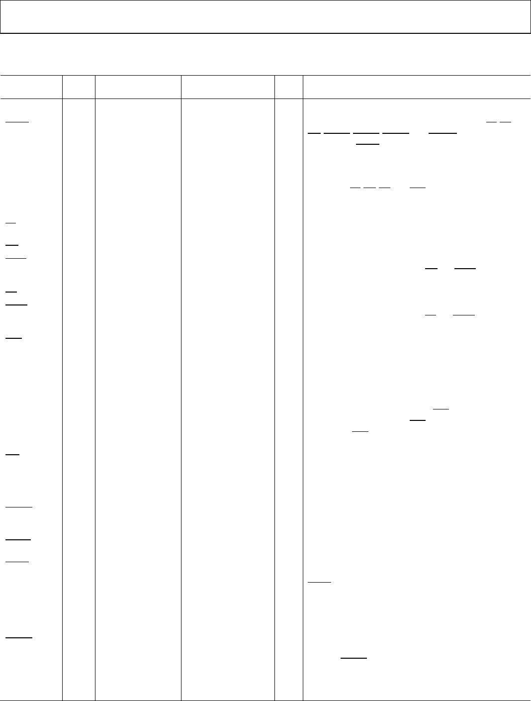
Table 17.
Mnemonic
Pins
Used 121-Lead Package 144-Lead Package I/O Description
MCLK 1 L9 L12 I System Input Clock. For details, see the PLL section.
Maximum input frequency on MCLK is 74.25 MHz.
RESET
1 L7 L11 I Reset. Causes the ADV202 to immediately reset.
CS
,
RD
,
WE
,
DACK0
,
DACK1
,
DREQ0
, and
DREQ1
must be held
high when a
RESET
is applied.
HDATA[15:0]
16
D4 to D1, C5 to C3,
B5, B4, C2, B3 to B1,
A2, A6 to A5
F4, E1 to E3, D1 to D3,
C1 to C3, B1 to B3, A2,
A3, A4
I/O
Host Data Bus. With HDATA[23:16], [27:24], [31:28], these
pins make up the 32-bit wide host data bus.
The async host interface is interfaced together with
ADDR[3:0],
CS
,
WE
,
RD
, and
ACK
. Unused HDATA pins
should be pulled down via a 10 kΩ resistor.
ADDR[3:0]
4
H11, K8, H10, J9 J12, J11, J10, H12 I
Address Bus for the Host Interface.
CS
1 J8 H11 I Chip Select. This signal is used to qualify addressed read
and write access to the ADV202 using the host interface.
WE
1 J7 H10 I Write Enable Used with the Host Interface.
RDFB
Read Enable When Fly-By DMA Is Enabled.
Note: Simultaneous assertion of
WE
and
DACK
low activates
the HDATA bus, even if the DMA channels are disabled.
RD
1 H9 G12 I Read Enable. Used with the host interface.
WEFB
Write Enable When Fly-By DMA Is Enabled.
Note: Simultaneous assertion of
RD
and
DACK
low activates
the HDATA bus, even if the DMA channels are disabled.
ACK
1 H8 G11 O Acknowledge. Used for direct register accesses. This signal
indicates that the last register access was successful.
Note: Due to synchronization issues, control and status
register accesses can incur an additional delay, so the host
software should wait for acknowledgment from the ADV202.
Accesses to the FIFOs (external DMA modes), on the other
hand, are guaranteed to occur immediately, if space is
available, and should not wait for
ACK
, if the timing
constraints are observed. If
ACK
is shared with more than
one device,
ACK
should be connected to a pull-up resistor
(10 kΩ) and the PLL_HI register, Bit 4, must be set to 1.
IRQ
1 G10 G10 O Interrupt. This pin indicates that the ADV202 requires the
attention of the host processor. This pin can be
programmed to indicate the status of the internal
interrupt conditions within the ADV202. The interrupt
sources are enabled via bits in Register EIRQIE.
DREQ0
1 F8 F12 O Data Request for External DMA Interface. Indicates that
the ADV202 is ready to send/receive data to/from the FIFO
assigned to DMA Channel 0.
FSRQ0
O Used in DCS-DMA Mode. Service request from the FIFO
assigned to Channel 0 (asynchronous mode).
VALID
O Valid Indication for JDATA Input/Output Stream. Polarity
of this pin is programmable in the EDMOD0 register.
VALID
is always an output.
CFG[1] I Boot Mode Configuration. This pin is read on reset to
determine the boot configuration of the on-board
processor. The pin should be tied to IOVDD or DGND
through a 10 kΩ resistor.
DACK0
1 F9 F11 I Data Acknowledge for External DMA Interface. Signal
from the host CPU, which indicates that the data transfer
request (
DREQ0
) has been acknowledged and data
transfer can proceed. This pin must be held high at all
times if the DMA interface is not used, even if the DMA
channels are disabled.


