Data Sheet ADV202
Rev. D | Page 33 of 40
Table 25. Maximum Supported Tile Width for Data Input on HDATA and VDATA Buses
Compression Mode Input Format Tile/Precinct Maximum Width
9/7i Single-component 2048
9/7i Two-component 1024 each
9/7i Three-component 1024 (Y)
5/3i Single-component 4096
5/3i Two-component 2048 (each)
5/3i Three-component 2048 (Y)
5/3r Single-component 4096
5/3r Two-component 2048
5/3r Three-component 1024
ADV202 Data Sheet
Rev. D | Page 34 of 40
APPLICATIONS
This section describes typical video applications for the
ADV202 JPEG2000 video processor.
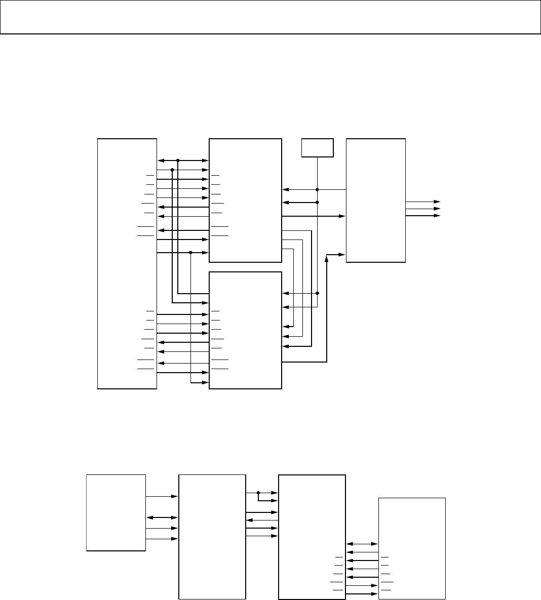
ENCODE—MULTICHIP MODE
Due to the data input rate limitation (see Table 24), an 1080i
application requires at least two ADV202s to encode or decode
full-resolution 1080i video. In encode mode, the ADV202
accepts Y and CbCr data on separate buses. The input data must
be in EAV/SAV format. An encode example is shown in Figure 24.
In decode mode, a master/slave configuration (as shown in
Figure 25) or a slave/slave configuration can be used to
synchronize the outputs of the two ADV202s. See AN-796
ADV202 Multichip Application application note for details on
how to configure the ADV202s in a multichip application.
Applications that have two separate VDATA outputs sent to an
FPGA or buffer before they are sent to an encoder do not
require synchronization at the ADV202 outputs
04723-002
DATA[31:0] HDATA[31:0]
ADDR[3:0] ADDR[3:0]
CS CS
RD RD
WR WE
ACK ACK
IRQ
CS
RD
WR
ACK
IRQ
DREQ
DACK
IRQ
DREQ DREQ
FIELD
VSYNC
HSYNC
DACK DACK
G I/O SCOMM[5]
VCLK
1080i
VIDEO IN
MCLK
VDATA[11:2]
32-BIT HOST CPU
10-BIT SD/HD
VIDEO
DECODER
ADV202
_1_SLAVE
SCOMM[5]
HDATA[31:0]
ADDR[3:0]
CS
RD
WE
ACK
IRQ
FIELD
VSYNC
HSYNC
DREQ
DACK
VCLK
MCLK
VDATA[11:2]
ADV202
_2_SLAVE
LLC
Y[9:0]
C[9:0]
CbCr
CbCr
Y
Figure 24. EncodeMultichip Application
Data Sheet ADV202
Rev. D | Page 35 of 40
DECODE—MULTICHIP MASTER/SLAVE
In a master/slave configuration, it is expected that the master HVF
outputs are connected to the slave HVF inputs and that each
SCOMM[5] pin is connected to the same GPIO on the host.
In a slave/slave configuration, the common HVF for both
ADV202s is generated by an external house sync, and each
SCOMM[5] is connected to the same GPIO output on the host.
SWIRQ1, Software Interrupt 1 in the EIRQIE register, must be
unmasked on both devices to enable multichip mode.
04723-003
DATA[31:0] HDATA[31:0]
ADDR[3:0] ADDR[3:0]
CS CS
RD
RD
WR
WE
ACK
ACK
IRQ
CS
RD
WR
ACK
IRQ
DREQ
DACK
IRQ
DREQ
DREQ
FIELD
VSYNC
HSYNC
DACK
DACK
G I/O SCOMM[5]
VCLK
1080i
VIDEO OUT
MCLK
VDATA[11:2]
32-BIT HOST CPU
10-BIT SD/HD
VIDEO
ENCODER
ADV202
_1_MASTER
SCOMM[5]
HDATA[31:0]
ADDR[3:0]
CS
RD
WE
ACK
IRQ
FIELD
VSYNC
HSYNC
DREQ
DACK
VCLK
MCLK
VDATA[11:2]
ADV202
CLKIN
Y[9:0]
C[9:0]
CbCr
CbCr
Y Y
74.25MHz
OSC
Figure 25. DecodeMultichip Master/Slave Application
DIGITAL STILL CAMERA/CAMCORDER
Figure 26 is a typical configuration for a digital camera or camcorder.
04723-004
D[9:0]
10
DATA INPUTS[9:0]
MCLK
VCLK
VFRM
VRDY
VSTRB
VDATA[15:6]
SDATA SERIAL DATA
SCK SERIAL CLK
SL SERIAL EN
AD9843A FPGA
16-BIT
HOST CPU
ADV202
DATA[15:0]HDATA[15:0]
ADDR[3:0]ADDR[3:0]
CSCS
RD
RD
WEWE
ACKACK
IRQIRQ
Figure 26. Digital Still Camera/Camcorder Encode Application for 10-Bit Pixel Data Using Raw Pixel Mode

ADV202BBCZ-150

Mfr. #:
Manufacturer:
Analog Devices Inc.
Description:
Interface - CODECs JPEG 2000 Video IC 150 MHz
Lifecycle:
New from this manufacturer.
Delivery:
DHL FedEx Ups TNT EMS
Payment:
T/T Paypal Visa MoneyGram Western Union