ADV202 Data Sheet
Rev. D | Page 30 of 40
INDIRECT REGISTERS
In certain modes, such as custom-specific input format or HIPI
mode, indirect registers must be accessed by the user through
the use of the IADDR and IDATA registers. The indirect
register address space starts at Internal Address 0xFFFF0000.
Both 32-bit and 16-bit hosts can access the indirect registers.
32-bit hosts use the IADDR and IDATA registers, while the
16-bit hosts use IADDR, IDATA, and the stage register.
For additional information on accessing and configuring these
registers, see the ADV202 User’s Guide.
Table 20. Indirect Registers
Address Name Description
0xFFFF0400 PMODE1 Pixel/Video Format
0xFFFF0404 COMP_CNT_STATUS Horizontal Count
0xFFFF0408 LINE_CNT_STATUS Vertical Count
0xFFFF040C XTOT Total Samples per Line
0xFFFF0410 YTOT Total Lines per Frame
0xFFFF0414 F0_START Start Line of Field 0 [F0]
0xFFFF0418 F1_START Start Line of Field 1 [F1]
0xFFFF041C V0_START Start of Active Video Field 0 [F0]
0xFFFF0420 V1_START Start of Active Video Field 1 [F1]
0xFFFF0424 V0_END End of Active Video Field 0 [F0]
0xFFFF0428 V1_END End of Active Video Field 1 [F1]
0xFFFF042C PIXEL_START Horizontal Start of Active Video
0xFFFF0430 PIXEL_END Horizontal End of Active Video
0xFFFF0440 MS_CNT_DEL Master/Slave Delay
0xFFFF0444 Reserved Reserved
0xFFFF0448 PMODE2 Pixel Mode 2
0xFFFF044C VMODE Video Mode
0xFFFF1408 EDMOD0 External DMA Mode Register 0
0xFFFF140C EDMOD1 External DMA Mode Register 1
0xFFFF1410 FFTHRP FIFO Threshold for Pixel FIFO
0xFFFF1414 Reserved Reserved
0xFFFF1418 Reserved Reserved
0xFFFF141C FFTHRC FIFO Threshold for CODE FIFO
0xFFFF1420 FFTHRA FIFO Threshold for ATTR FIFO
0xFFFF1428 to 0xFFFF14FC Reserved Reserved
Data Sheet ADV202
Rev. D | Page 31 of 40
PLL
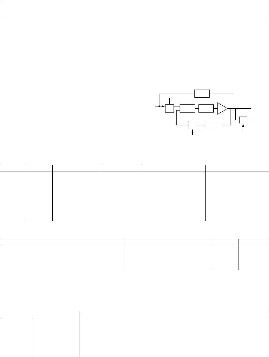
The ADV202 uses the PLL_HI and PLL_LO direct registers to
configure the PLL. Any time the PLL_LO register is modified,
the host must wait at least 20 µs before reading or writing to any
other register. If this delay is not implemented, erratic behavior
could result.
The PLL can be programmed to have any possible final
multiplier value as long as
JCLK > 50 MHz and < 150 MHz (144-lead version).
JCLK > 50 MHz and < 135 MHz (144-lead version).
JCLK > 50 MHz and < 115 MHz (121-lead version).
HCLK < 108 MHz (144-lead, 150 MHz version).
HCLK < 100 MHz (144-lead, 135 MHz version).
HCLK < 81 MHz (121-lead version).
JCLK ≥ 2 × VCLK for single-component input.
JCLK ≥ 2 × VCLK for YCrCb [4:2:2] input.
In JDATA mode (JDATA), JCLK must be 4 × MCLK or
higher.
For de-interlaced modes, JCLK must be ≥ 4 × MCLK.
The maximum burst frequency for external DMA modes is
0.36 JCLK.
For MCLK frequencies greater than 50 MHz, the input
clock divider must be enabled, that is, IPD set to 1.
IPD cannot be enabled for MCLK frequencies below 20 MHz.
To achieve the lowest power consumption, an MCLK frequency
of 27 MHz is recommended for a standard definition CCIR656
input. The PLL circuit is recommended to have a multiplier of 3.
This sets JCLK and HCLK to 81 MHz.
04723-009
LPF
PHASE
DETECT
VCO
JCLK
HCLK
2
HCLKD
PLLMULT 2
LFB
2
IPD
BYPASS
MCLK
Figure 23. PLL Architecture and Control Functions
Table 21. Recommended PLL Register Settings
IPD LFB PLLMULT HCLKD HCLK JCLK
0 0 N 0 N × MCLK N × MCLK
0 0 N 1 N × MCLK/2 N × MCLK
0 1 N 0 2 × N × MCLK 2 × N × MCLK
0 1 N 1 N × MCLK 2 × N × MCLK
1 0 N 0 N × MCLK/2 N × MCLK/2
1 0 N 1 N × MCLK/4 N × MCLK/2
1 1 N 0 N × MCLK N × MCLK
1 1 N 1 N × MCLK/2 N × MCLK
Table 22. Recommended Values for PLL_HI and PLL_LO Registers
Video Standard CLKIN Frequency on MCLK PLL_HI PLL_LO
SMPTE125M or ITU-R.BT656 (NTSC or PAL) 27 MHz 0x0008 0x0004
SMPTE293M (525p) 27 MHz 0x0008 0x0004
ITU-R.BT1358 (625p) 27 MHz 0x0008 0x0004
SMPTE274M (1080i) 74.25 MHz 0x0008 0x0084
HARDWARE BOOT
The boot mode can be configured via hardware using the CFG pins or via software (see the ADV202 User’s Guide). The first boot mode
after power-up is set by the CFG pins. Only Boot Mode 2, Boot Mode 4, and Boot Mode 6, described in Table 23, are available via hardware.
Table 23. Hardware Boot Modes
Boot Mode Settings Description
Hardware Boot
Mode 2
CFG[1] tied high,
CFG[2] tied low
No-Boot Host Mode. ADV202 does not boot, but all internal registers and memory are accessible
through normal host I/O operations.
For details, see the ADV202 User’s Guide and the Getting Started with the ADV202 application note.
Hardware Boot
Mode 4
CFG[1] tied low,
CFG[2] tied high
SoC Boot Mode.
Hardware Boot
Mode 6
CFG[1] and CFG[2]
tied high
Reserved.
ADV202
Rev. D | Page 32 of 40
VIDEO INPUT FORMATS
The ADV202 supports a wide variety of formats for
uncompressed video and still image data. The actual interface
and bus modes selected for transferring uncompressed data
dictates the allowed size of the input data and the number of
samples transferred with each access.
The host interface can support 8-, 10-, 12-, 14-, and 16-bit data
formats. The video interface can support video data or still image
data input/output. Supported formats are 8-, 10-, 12-, or 16-bit
single component or YCbCr 4:2:2 formats. See the ADV202
User’s Guide for details. All formats can support less precision
than provided by specifying the actual data width/precision in
the PMODE register.
The maximum allowable data input rate is limited by using
irreversible or reversible compression modes and the data width
(or precision) of the input samples. Use Table 24 and Table 25 to
determine the maximum data input rate.
Table 24. Maximum Pixel Data Input Rates
Interface
Compression
Mode Input Format
Input Rate Limit Active
Resolution (MSPS)
1
Approx Min Output Rate,
Compressed Data
2
(Mbps)
Approx Max Output Rate,
Compressed Data
3
(Mbps)
144-LEAD PACKAGE
HDATA Irreversible 8-bit data 45 [40] 130 200
Irreversible 10-bit data 45 [40] 130 200
Irreversible 12-bit data 45 [40] 130 200
Irreversible 16-bit data 45 [40] 130 200
Reversible 8-bit data 40 [36] 130 200
Reversible 10-bit data 32 [28] 130 200
Reversible 12-bit data 27 [24] 130 200
Reversible 14-bit data 23 [20] 130 200
VDATA Irreversible 8-bit data 65 [55] 130 200
Irreversible 10-bit data 65 [55] 130 200
Irreversible 12-bit data 65 [55] 130 200
Reversible 8-bit data 40 [34] 130 200
Reversible 10-bit data 32 [28] 130 200
Reversible 12-bit data 27 [23] 130 200
121-LEAD PACKAGE
HDATA Irreversible 8-bit data 34 98 150
Irreversible 10-bit data 34 98 150
Irreversible 12-bit data 34 98 150
Irreversible 16-bit data 34 98 150
Reversible 8-bit data 30 98 150
Reversible 10-bit data 24 98 150
Reversible 12-bit data 20 98 150
Reversible 14-bit data 17 98 150
VDATA Irreversible 8-bit data 48 98 150
Irreversible 10-bit data 48 98 150
Irreversible 12-bit data 48 98 150
Reversible 8-bit data 30 98 150
Reversible 10-bit data 24 98 150
Reversible 12-bit data 20 98 150
1
Input rate limits for HDATA can be less for certain applications depending on input picture size and content, host interface settings, and DMA transfer settings. Values
in brackets refer to the 135 MHz speed grade version of the ADV202.
2
Minimum guaranteed sustained output rate or minimum sustainable compression rate (input rate/minimum peak output rate).
3
Maximum peak output rate, or output rate above this value is not possible .

ADV202BBCZ-150

Mfr. #:
Manufacturer:
Analog Devices Inc.
Description:
Interface - CODECs JPEG 2000 Video IC 150 MHz
Lifecycle:
New from this manufacturer.
Delivery:
DHL FedEx Ups TNT EMS
Payment:
T/T Paypal Visa MoneyGram Western Union