Data Sheet ADV202
Rev. D | Page 27 of 40
ADV202 INTERFACE
There are several possible modes to interface to the ADV202 using
the VDATA bus and the HDATA bus or the HDATA bus alone.
VIDEO INTERFACE (VDATA BUS)
The video interface can be used in applications in which
uncompressed pixel data is on a separate bus from compressed
data. For example, it is possible to use the VDATA bus to input
uncompressed video while using the HDATA bus to output the
compressed data. This interface is ideal for applications
requiring very high throughput such as live video capture.
Optionally, the ADV202 can compress ITU.R-BT656 resolution
video on a field-by-field basis or on a two-fields-combined
basis, which yields significantly more efficient compression
performance. Additionally, high definition digital video such as
SMPTE274M (1080i) is supported using two or more ADV202
devices.
The video interface can support video data or still image data
input/output, 8-, 10-, and 12-bit single or multiplexed
components. The VDATA interface supports digital video in
YCbCr format or single component format. YCbCr data must
be in 4:2:2 format.
Video data can be input/output in several different modes on
the VDATA bus, as described in Table 18. In all these modes,
the pixel clock must be input on the VCLK pin.
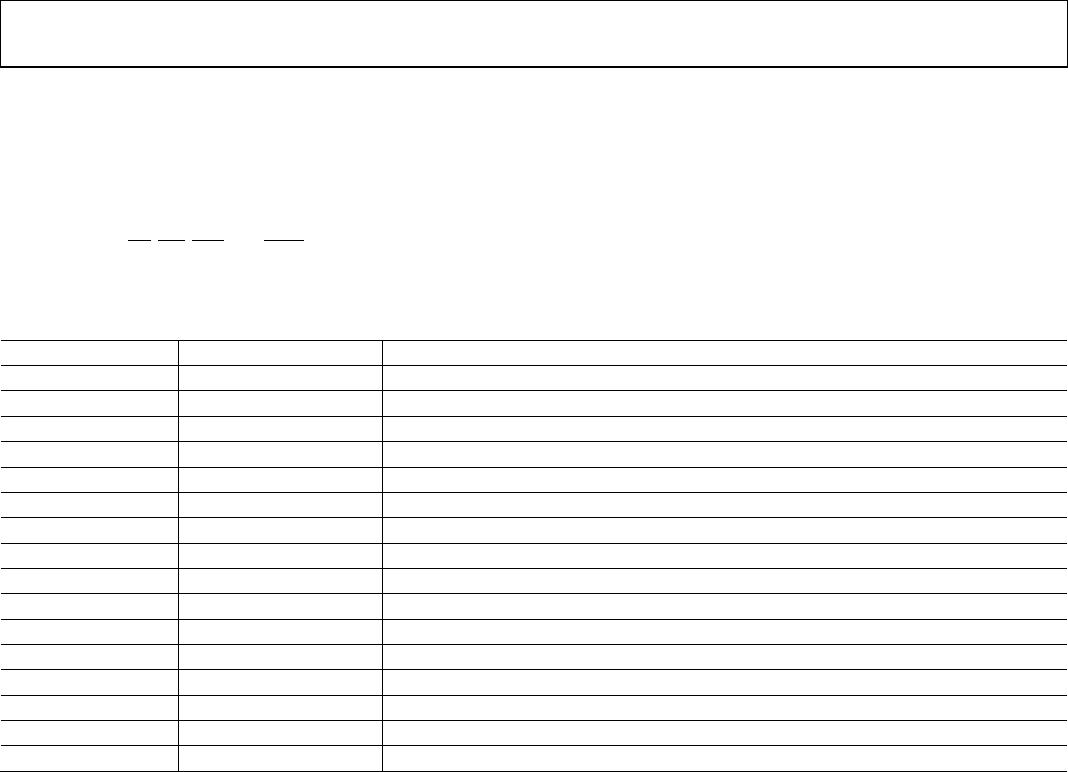
Table 18. Video Input/Output Modes
Mode Description
EAV/SAV Accepts video with embedded EAV/SAV codes, where
the YCbCr data is interleaved onto a single bus.
HVF Accepts video data accompanied with separate H, V,
and F signals where YCbCr data is interleaved onto a
single bus.
Raw
Video
Used for still picture data and nonstandard video.
VFRM, VSTRB, and VRDY are used to program the
dimensions of the image.
HOST INTERFACE (HDATA BUS)
The ADV202 can connect directly to a wide variety of host
processors and ASICs using an asynchronous SRAM-style
interface, DMA accesses, or streaming mode (JDATA) interface.
The ADV202 supports 16- and 32-bit buses for control and
8-, 16-, and 32-bit buses for data transfer.
The control and data channel bus widths can be specified
independently, which allows the ADV202 to support applica-
tions that require control and data buses of different widths.
The host interface is used for configuration, control, and status
functions, as well as for transferring compressed data streams. It
can be used for uncompressed data transfers in certain modes.
The host interface can be shared by as many as four concurrent
data streams in addition to control and status communications.
The data streams are
Uncompressed tile data (for example, still image data)
Fully encoded JPEG2000 code stream (or unpackaged code
blocks)
Code-block attributes
The ADV202 uses big endian byte alignment for 16- and 32-bit
transfers. All data is left-justified (MSB).
Pixel Input on the Host Interface
Pixel input on the host interface supports 8-, 10-, 12-, 14-, and
16-bit raw pixel data formats. It can be used for pixel (still
image) input/output or compressed video output. Because there
are no timing codes or sync signals associated with the input
data on the host interface, dimension registers and internal
counters are used and must be programmed to indicate the start
and end of the frame. See the technical note on using HIPI
mode for details on how to use the ADV202 in this mode.
Host Bus Configuration
For maximum flexibility, the host interface provides several
configurations to meet particular system requirements. The
default bus mode uses the same pins to transfer control, status,
and data to and from the ADV202. In this mode, the ADV202
can support 16- and 32-bit control transfers and 8-, 16-, and
32-bit data transfers. The size of these buses can be selected
independently, allowing, for example, a 16-bit microcontroller
to configure and control the ADV202 while still providing
32-bit data transfers to an ASIC or external memory system.
DIRECT AND INDIRECT REGISTERS
To minimize pin count and cost, the number of address pins has
been limited to four, which yields a total direct address space of
16 locations. These locations are most commonly used by the
external controller and are, therefore, accessible directly. All
other registers in the ADV202 can be accessed indirectly
through the IADDR and IDATA registers.
CONTROL ACCESS REGISTERS
With the exception of the indirect address and data registers
(IADDR and IDATA), all control/status registers in the ADV202
are 16 bits wide and are half-word (16-bit) addressable only.
When 32-bit host mode is enabled, the upper 16 bits of the
HDATA bus are ignored on writes and return all 0s on reads of
16-bit registers.
ADV202 Data Sheet
Rev. D | Page 28 of 40
PIN CONFIGURATION AND BUS SIZES/MODES
The ADV202 provides a wide variety of control and data
configurations, which allows it to be used in many applications
with little or no glue logic. The following modes are configured
using the BUSMODE register. In the following descriptions,
host refers to normal addressed accesses (
CS
/
RD
/WR/ADDR)
and data refers to external DMA accesses (
DREQ
/
DACK
).
32-Bit Host/32-Bit Data
In this mode, the HDATA[31:0] pins provide full 32-bit wide data
accesses to PIXEL, CODE, and ATTR FIFOs. The expanded
video interface (VDATA) is not available in this mode.
16-Bit Host/32-Bit Data
This mode allows a 16-bit host to configure and communicate
with the ADV202 while still allowing 32-bit accesses to the
PIXEL, CODE, and ATTR FIFOs using the external DMA
capability.
All addressed host accesses are 16 bits and, therefore, use only
the HDATA[15:0] pins. The HDATA[31:16] pins provide the
additional 16 bits necessary to support the 32-bit external DMA
transfers to and from the FIFOs only. The expanded video
interface (VDATA) is not available in this mode.
16-Bit Host/16-Bit Data
This mode uses 16-bit transfers, if used for host or external
DMA data transfers. This mode allows for the use of the
extended pixel interface modes.
16-Bit Host/8-Bit Data (JDATA Bus Mode)
This mode provides separate data input/output and host
control interface pins. Host control accesses are 16 bits and use
HDATA[15:0], while the dedicated data bus uses JDATA[7:0].
JDATA uses a valid/hold synchronous transfer protocol. The
direction of the JDATA bus is determined by the mode of the
ADV202. If the ADV202 is encoding (compression), JDATA[7:0]
is an output. If the ADV202 is decoding (decompression),
JDATA[7:0] is an input. Host control accesses remain
asynchronous (also refer to the JDATA Mode section).
STAGE REGISTER
Because the ADV202 contains both 16-bit and 32-bit registers
and its internal memory is mapped as 32-bit data, a mechanism
has been provided to allow 16-bit hosts to access these registers
and memory locations using the stage register (STAGE).
STAGE is accessed as a 16-bit register using HDATA[15:0].
Prior to writing to the desired register, the stage register must be
written with the upper (most significant) half-word.
When the host subsequently writes the lower half-word to the
desired control register, HDATA is combined with the previously
staged value to create the required 32-bit value that is written.
When a register is read, the upper (most significant) half-word
is returned immediately on HDATA and the lower half-word
can be retrieved by reading the stage register on a subsequent
access. For details on using the stage register, see the ADV202
User’s Guide.
Note that the stage register does not apply to the three data
channels (PIXEL, CODE, and ATTR). These channels are
always accessed at the specified data width and do not require
the use of the stage register.
JDATA MODE
JDATA mode is typically used only when the dedicated video
interface (VDATA) is also enabled. This mode allows code
stream data (compressed data compliant with JPEG2000) to be
input or output on a single dedicated 8-bit bus (JDATA[7:0]).
The bus is always an output during compression operations
and is an input during decompression.
A 2-pin handshake is used to transfer data over this synchro-
nous interface. VALID is used to indicate that the ADV202 is
ready to provide or accept data and is always an output. HOLD
is always an input and is asserted by the host if it cannot accept/
provide data. For example, JDATA mode allows real-time
applications, in which pixel data is input over the VDATA bus
while the compressed data stream is output over the JDATA bus.
EXTERNAL DMA ENGINE
The external DMA interface is provided to enable high
bandwidth data I/O between an external DMA controller and
the ADV202 data FIFOs. Two independent DMA channels can
each be assigned to any one of the three data stream FIFOs
(PIXEL, CODE, or ATTR).
The controller supports asynchronous DMA using a data-
request/data-acknowledge (
DREQ
/
DACK
) protocol in either
single or burst access modes. Additional functionality is provided
for single address compatibility (fly-by) and dedicated chip
select (DCS) modes.
ADV202
Rev. D | Page 29 of 40
INTERNAL REGISTERS
This section describes the internal registers of the ADV202.
DIRECT REGISTERS
The ADV202 has 16 direct registers, as listed in Table 19.
The direct registers are accessed over the ADDR[3:0],
HDATA[31:0],
CS
,
RD
,
WR
, and
ACK
pins.
The host must first initialize the direct registers before any
application-specific operation can be implemented.
For additional information on accessing and configuring these
registers, see the ADV202 User’s Guide.
Table 19. Direct Registers
Address Name Description
0x00 PIXEL Pixel FIFO Access Register
0x01 CODE Compressed Code Stream Access Register
0x02 ATTR Attribute FIFO Access Register
0x03 Reserved Reserved
0x04 CMDSTA Command Stack
0x05 EIRQIE External Interrupt Enabled
0x06 EIRQFLG External Interrupt Flags
0x07 SWFLAG Software Flag Register
0x08 BUSMODE Bus Mode Configuration Register
0x09 MMODE Miscellaneous Mode Register
0x0A STAGE Staging Register
0x0B IADDR Indirect Address Register
0x0C IDATA Indirect Data Register
0x0D BOOT Boot Mode Register
0x0E PLL_HI PLL Control RegisterHigh Byte
0x0F PLL_LO PLL Control RegisterLow Byte

ADV202BBCZ-150

Mfr. #:
Manufacturer:
Analog Devices Inc.
Description:
Interface - CODECs JPEG 2000 Video IC 150 MHz
Lifecycle:
New from this manufacturer.
Delivery:
DHL FedEx Ups TNT EMS
Payment:
T/T Paypal Visa MoneyGram Western Union