AMIS−30522, NCV70522
http://onsemi.com
8
Table 6. AC PARAMETERS (The AC Parameters are Given for V
BB
and Temperature in Their Operating Ranges)
Symbol
Pin(s) Parameter Remark/Test Conditions Min Typ Max Unit
INTERNAL OSCILLATOR
f
osc
Frequency of Internal Oscillator 3.6 4.0 4.4 MHz
MOTORDRIVER
f
PWM
MOTxx
PWM Frequency
Frequency Depends Only on
Internal Oscillator
20.8 22.8 24.8 kHz
Double PWM Frequency 41.6 45.6 49.6 kHz
f
d
PWM Jitter Depth (Note 13) 10 % f
PWM
tb
rise
MOTxx
Turn−On Voltage Slope, 10% to 90%
(Note 13)
EMC[1:0] = 00 150
V/ms
EMC[1:0] = 01 100
V/ms
EMC[1:0] = 10 50
V/ms
EMC[1:0] = 11 25
V/ms
tb
fall
MOTxx
Turn−off Voltage Slope, 90% to 10%
(Note 13)
EMC[1:0] = 00 150
V/ms
EMC[1:0] = 01 100
V/ms
EMC[1:0] = 10 50
V/ms
EMC[1:0] = 11 25
V/ms
DIGITAL OUTPUTS
t
H2L
DO
ERR
Output Falltime from V
inH
to V
inL
Capacitive Load 400 pF and
Pullup Resistor of 1.5 kW
50 ns
CHARGE PUMP
f
CP
CPN
CPP
Charge Pump Frequency 250 kHz
t
CPU
MOTxx Startup Time of Charge Pump (Note 14) Spec External Components 5.0 ms
CLR FUNCTION
t
CLR
CLR Minimum Time for Hard Reset 100
ms
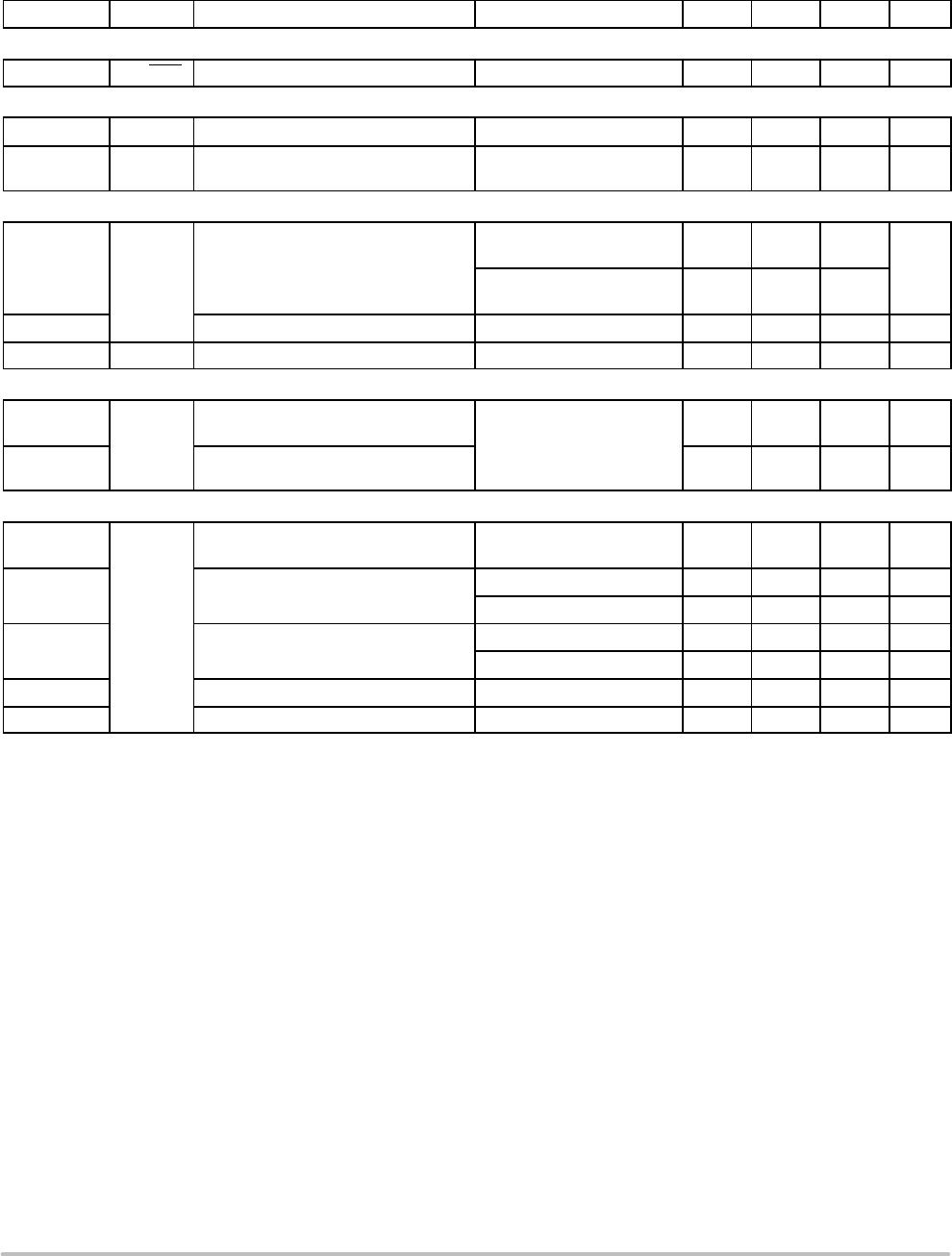
NXT FUNCTION
t
NXT_HI
NXT
NXT Minimum, High Pulse Width See Figure 4 2.0
ms
t
NXT_LO
NXT Minimum, Low Pulse Width See Figure 4 2.0
ms
t
DIR_SET
NXT Hold Time, Following
Change of DIR
See Figure 4 2.0
ms
t
DIR_HOLD
NXT Hold Time, Before Change of DIR See Figure 4 2.0
ms
POWER UP
t
PU
PORB/
WD
Power−Up Time
V
BB
= 12 V, I
LOAD
= 50 mA,
C
LOAD
= 220 nF
110
ms
t
PD
Power−Down Time external conditions ms
t
POR
Reset Duration 100 ms
t
RF
Reset Filter Time 1.0
ms
WATCHDOG
t
WDTO
Watchdog Time Out Interval 32 512 ms
t
WDPR
Prohibited Watchdog
Acknowledge Delay
2.0 ms
13.Characterization Data Only
14.Guaranteed by design.