LTC4066/LTC4066-1
25
4066fc
APPLICATIONS INFORMATION
to make thermal contact between the Exposed Pad on the
backside of the package and the copper board will result
in thermal resistances far greater than 37°C/W. As an
example, a correctly soldered LTC4066/LTC4066-1 can
deliver over 1A to a battery from a 5V supply at room
temperature. Without a backside thermal connection, this
number could drop to less than 500mA.
Furthermore, Pins 6 and 7 are “true No Connect” pins.
Therefore, they can be used to improve the amount of
metal used to connect to Pin 5 or Pin 8.
V
IN
and Wall Adapter Bypass Capacitor
Many types of capacitors can be used for input bypassing.
However, caution must be exercised when using multilayer
ceramic capacitors. Because of the self resonant and high
Q characteristics of some types of ceramic capacitors, high
voltage transients can be generated under some start-up
conditions, such as connecting the charger input to a hot
power source. For more information, refer to Application
Note 88.
Stability
The constant-voltage mode feedback loop is stable without
any compensation when a battery is connected. However,
a 4.7μF capacitor with a 1Ω series resistor to GND is
recommended at the BAT pin to keep ripple voltage low
when the battery is disconnected.
LTC4066/LTC4066-1
26
4066fc
PACKAGE DESCRIPTION
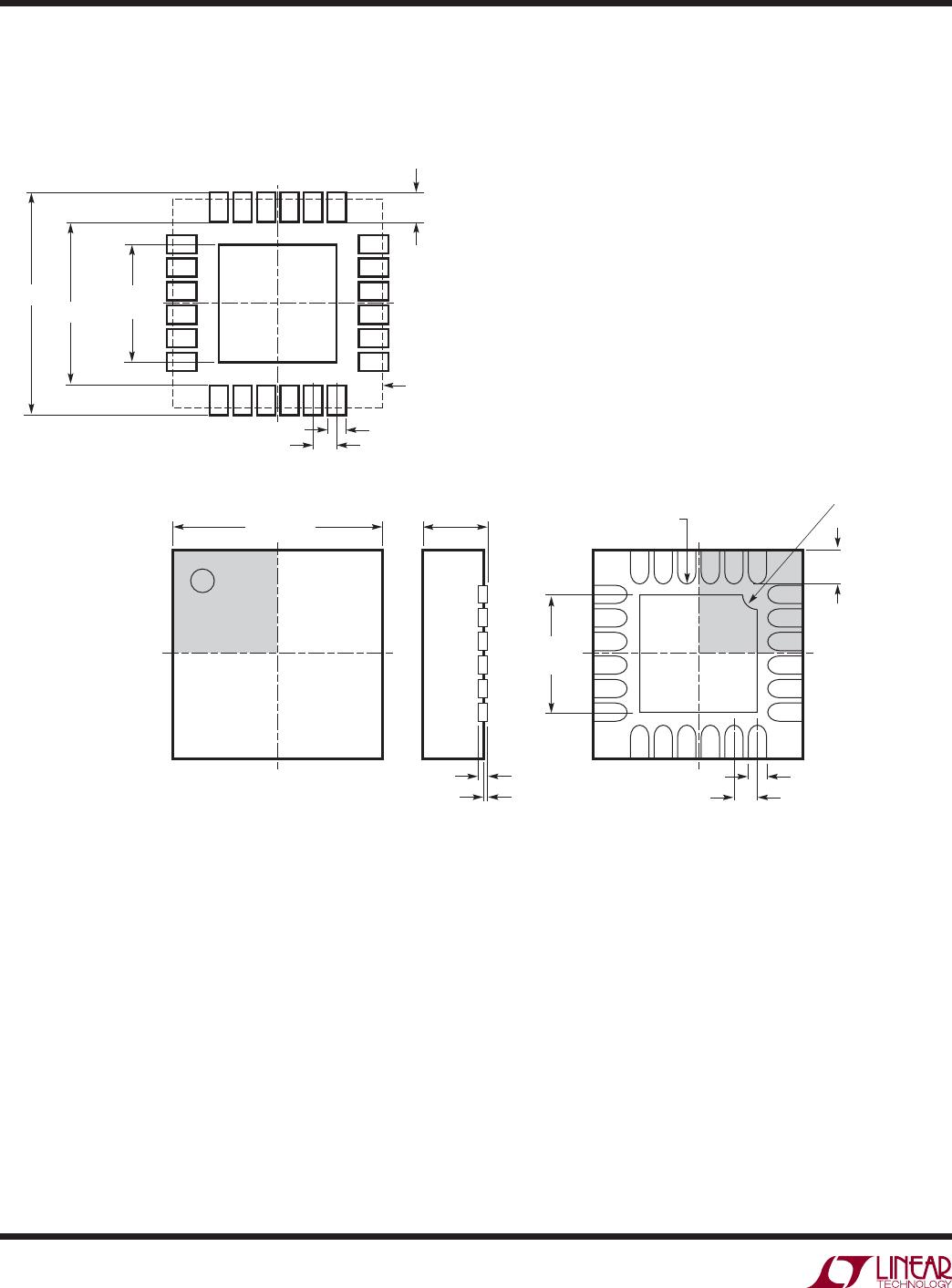
UF Package
24-Lead Plastic QFN (4mm × 4mm)
(Reference LTC DWG # 05-08-1697)
4.00 p 0.10
(4 SIDES)
NOTE:
1. DRAWING PROPOSED TO BE MADE A JEDEC PACKAGE OUTLINE MO-220 VARIATION (WGGD-X)—TO BE APPROVED
2. DRAWING NOT TO SCALE
3. ALL DIMENSIONS ARE IN MILLIMETERS
4. DIMENSIONS OF EXPOSED PAD ON BOTTOM OF PACKAGE DO NOT INCLUDE
MOLD FLASH. MOLD FLASH, IF PRESENT, SHALL NOT EXCEED 0.15mm ON ANY SIDE, IF PRESENT
5. EXPOSED PAD SHALL BE SOLDER PLATED
6. SHADED AREA IS ONLY A REFERENCE FOR PIN 1 LOCATION
ON THE TOP AND BOTTOM OF PACKAGE
PIN 1
TOP MARK
(NOTE 6)
0.40 p 0.10
2423
1
2
BOTTOM VIEW—EXPOSED PAD
2.45 p 0.10
(4-SIDES)
0.75 p 0.05
R = 0.115
TYP
0.25 p 0.05
0.50 BSC
0.200 REF
0.00 – 0.05
(UF24) QFN 0105
RECOMMENDED SOLDER PAD PITCH AND DIMENSIONS
0.70 p0.05
0.25 p0.05
0.50 BSC
2.45 p 0.05
(4 SIDES)
3.10 p 0.05
4.50 p 0.05
PACKAGE OUTLINE
PIN 1 NOTCH
R = 0.20 TYP OR
0.35 s 45o CHAMFER
LTC4066/LTC4066-1
27
4066fc
Information furnished by Linear Technology Corporation is believed to be accurate and reliable.
However, no responsibility is assumed for its use. Linear Technology Corporation makes no representa-
tion that the interconnection of its circuits as described herein will not infringe on existing patent rights.
PACKAGE DESCRIPTION
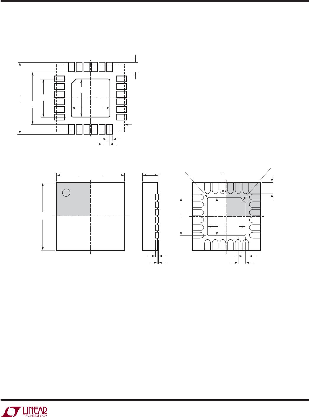
PF Package
24-Lead Plastic UTQFN (4mm × 4mm)
(Reference LTC DWG # 05-08-1748 Rev Ø)
4.00 p 0.10
4.00 p 0.10
NOTE:
1. DRAWING IS NOT A JEDEC PACKAGE OUTLINE
2. DRAWING NOT TO SCALE
3. ALL DIMENSIONS ARE IN MILLIMETERS
4. DIMENSIONS OF EXPOSED PAD ON BOTTOM OF PACKAGE DO NOT INCLUDE
MOLD FLASH. MOLD FLASH, IF PRESENT, SHALL NOT EXCEED 0.15mm ON ANY SIDE, IF PRESENT
5. EXPOSED PAD SHALL BE SOLDER PLATED
6. SHADED AREA IS ONLY A REFERENCE FOR PIN 1 LOCATION
ON THE TOP AND BOTTOM OF PACKAGE
PIN 1
TOP MARK
(NOTE 6)
0.40 p 0.10
2423
1
2
BOTTOM VIEW—EXPOSED PAD
2.45 p 0.10
2.50 REF
2.45 p 0.10
2.45 p 0.05
2.45 p 0.05
0.55 p 0.05
R = 0.115
TYP
R = 0.05
TYP
0.25 p 0.05
0.50 BSC
0.125 REF
0.00 – 0.05
(PF24) UTQFN 0107
RECOMMENDED SOLDER PAD PITCH AND DIMENSIONS
APPLY SOLDER MASK TO AREAS THAT ARE NOT SOLDERED
0.70 p0.05
0.25 p0.05
0.50 BSC
2.50 REF
3.10 p 0.05
4.50 p 0.05
PACKAGE OUTLINE
PIN 1 NOTCH
R = 0.20 TYP
OR 0.35 s 45o
CHAMFER

LTC4066EUF#PBF

Mfr. #:
Manufacturer:
Analog Devices / Linear Technology
Description:
Battery Management USB Power Manager and Li-Ion Charger
Lifecycle:
New from this manufacturer.
Delivery:
DHL FedEx Ups TNT EMS
Payment:
T/T Paypal Visa MoneyGram Western Union