LTC4066/LTC4066-1
7
4066fc
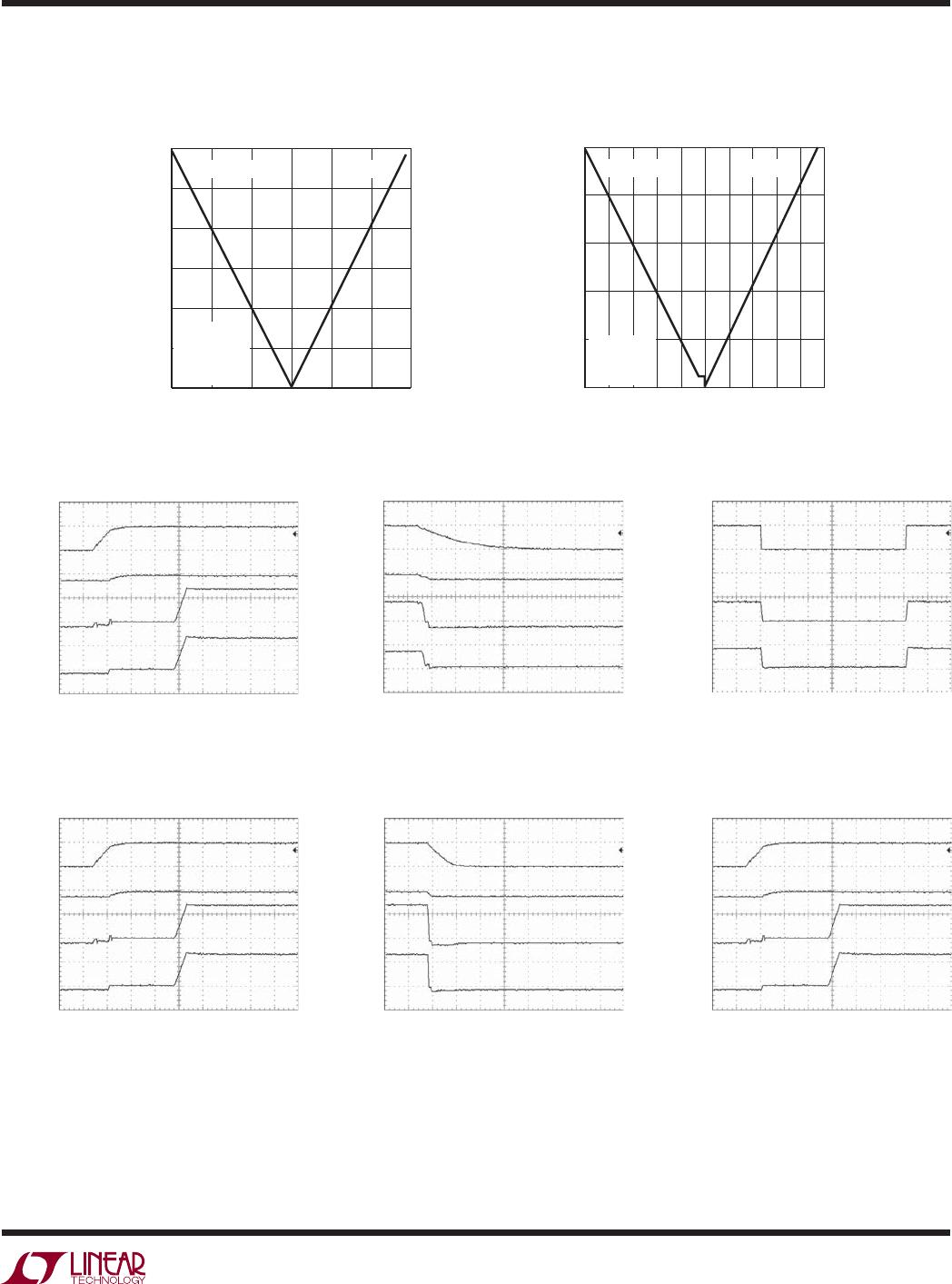
TYPICAL PERFORMANCE CHARACTERISTICS
I
STAT
Pin Current vs
Battery Current
I
STAT
Pin Current vs Battery
Current (Low Currents)
Input Connect Waveforms Input Disconnect Waveforms Response to HPWR
WALL Connect Waveforms,
V
IN
= 0V
Respond to Suspend
I
BAT
(mA)
–1500
0
I
ISTAT
(μA)
250
500
750
1000
1500
–1000
–500 0 500
4006 G19
1000 1500
1250
IDEAL DIODE CHARGING
V
BAT
= 4.2V
V
IN
= 5V
T
A
= 25°C
R
PROG
= 34k
I
BAT
(mA)
–10
I
ISTAT
(μA)
6
8
10
6
4066 G20
4
2
0
–8 –6 –4
–2 0
24 8
10
IDEAL DIODE CHARGING
V
BAT
= 4.2V
V
IN
= 5V
T
A
= 25°C
V
IN
5V/DIV
V
OUT
5V/DIV
I
IN
0.5A/DIV
I
BAT
0.5A/DIV
1ms/DIV
4066 G21
V
BAT
= 3.85V
I
OUT
= 100mA
V
IN
5V/DIV
V
OUT
5V/DIV
I
IN
0.5A/DIV
I
BAT
0.5A/DIV
1ms/DIV
4066 G22
V
BAT
= 3.85V
I
OUT
= 100mA
HPWR
5V/DIV
I
IN
0.5A/DIV
I
BAT
0.5A/DIV
1ms/DIV
4066 G23
V
BAT
= 3.85V
I
OUT
= 50mA
WALL Disconnect Waveforms,
V
IN
= 0V
WALL
5V/DIV
I
WALL
0.5A/DIV
V
OUT
5V/DIV
I
BAT
0.5A/DIV
1ms/DIV
4066 G24
V
BAT
= 3.85V
I
OUT
= 100mA
R
PROG
= 71.5k
WALL
5V/DIV
I
WALL
0.5A/DIV
V
OUT
5V/DIV
I
BAT
0.5A/DIV
1ms/DIV
4066 G25
V
BAT
= 3.85V
I
OUT
= 100mA
R
PROG
= 71.5k
SUSPEND
5V/DIV
I
IN
0.5A/DIV
V
OUT
5V/DIV
I
BAT
0.5A/DIV
1ms/DIV
4066 G26
V
BAT
= 3.85V
I
OUT
= 50mA
LTC4066/LTC4066-1
8
4066fc
PIN FUNCTIONS
TYPICAL PERFORMANCE CHARACTERISTICS
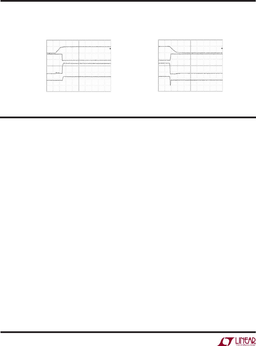
WALL Connect Waveforms,
V
IN
= 5V
WALL Disconnect Waveforms,
V
IN
= 5V
WALL
5V/DIV
I
WALL
0.5A/DIV
I
IN
0.5A/DIV
I
BAT
0.5A/DIV
1ms/DIV
4066 G27
V
BAT
= 3.85V
I
OUT
= 100mA
R
PROG
= 71.5k
WALL
5V/DIV
I
WALL
0.5A/DIV
I
IN
0.5A/DIV
I
BAT
0.5A/DIV
1ms/DIV
4066 G28
V
BAT
= 3.85V
I
OUT
= 100mA
R
PROG
= 71.5k
OUT (Pins 1, 3, 8): Voltage Output. This pin is used to
provide controlled power to a USB device from either
USB V
BUS
(IN) or the battery (BAT) when the USB is not
present. This pin can also be used as an input for battery
charging when the USB is not present and a wall adapter
is applied to this pin. OUT should be bypassed with at least
4.7μF to GND. Connect Pins 1, 3 and 8 with a resistance
no greater than 10mΩ.
BAT (Pins 2, 4, 5): Connect to a single cell Li-Ion battery.
This pin is used as an output when charging the battery, and
as an input when supplying power to OUT. When the OUT
pin potential drops below the BAT pin potential, an ideal
diode function connects BAT to OUT and prevents V
OUT
from
dropping more than 50mV below V
BAT
. A precision internal
resistor divider sets the fi nal fl oat (charging) potential on
this pin. The internal resistor divider is disconnected when
IN and OUT are in undervoltage lockout. Connect Pins 2,
4 and 5 with a resistance no greater than 10mΩ.
IN (Pin 9): Input Supply. Connect to USB supply, V
BUS
.
Input current to this pin is limited to either 20% or 100% of
the current programmed by the CLPROG pin as determined
by the state of the HPWR pin. The input current limit can
also be disabled by pulling CLDIS high. Charge current (to
BAT pin) supplied through the input is set to the current
programmed by the PROG pin but will be limited by the
input current limit if charge current is set greater than the
input current limit.
CLDIS (Pin 10): Current Limit Disable. This logic input
is used to disable the input current limit programmed by
CLPROG. A voltage greater than 1.2V on the pin will set
the current limit to I
IN(MAX)
(typically 2.6A). A weak pull-
down current is internally applied to this pin to ensure
it is low at power-up when the input is not being driven
externally.
SUSP (Pin 11): Suspend Mode Input. Pulling this pin
above 1.2V will disable the power path from IN to OUT. The
supply current from IN will be reduced to comply with the
USB specifi cation for Suspend mode. Both the ability to
charge the battery from OUT and the ideal diode function
(from BAT to OUT) will remain active. Suspend mode will
reset the charge timer if V
OUT
is less than V
BAT
while in
suspend mode. If V
OUT
is kept greater than V
BAT
, such as
when a wall adapter is present, the charge timer will not be
reset when the part is put in suspend. A weak pull-down
current is internally applied to this pin to ensure it is low
at power-up when the pin is not being driven externally.
LTC4066/LTC4066-1
9
4066fc
SHDN (Pin 12): Shutdown Input. Pulling this pin greater
than 1.2V will disable the entire part and place it in a low
supply current mode of operation. All power paths will be
disabled. A weak pull-down current is internally applied
to this pin to ensure it is enabled at power-up when the
pin is not being driven externally.
HPWR (Pin 13): High Power Select. This logic input is used
to control the input current limit. A voltage greater than
1.2V on the pin will set the input current limit to 100% of
the current programmed by the CLPROG pin. A voltage
less than 0.4V on the pin will set the input current limit
to 20% of the current programmed by the CLPROG pin.
A weak pull-down current is internally applied to this pin
to ensure it is low at power-up when the pin is not being
driven externally.
NTC (Pin 14): Input to the NTC Thermistor Monitoring
Circuits. Under normal operation, tie a thermistor from
the NTC pin to ground and a resistor of equal value from
NTC to V
NTC
. When the voltage on this pin is above 0.74
• V
VNTC
(Cold, 0°C) or below 0.29 • V
VNTC
(Hot, 50°C)
the timer is suspended, but not cleared, the charging is
disabled and the CHRG pin remains in its former state.
When the voltage on NTC comes back between 0.74 •
V
VNTC
and 0.29 • V
VNTC
, the timer continues where it left
off and charging is re-enabled if the battery voltage is
below the recharge threshold. There is approximately 3°C
of temperature hysteresis associated with each of the input
comparators. Connect the NTC pin to ground to disable
this feature. This will disable all of the LTC4066/LTC4066-1
NTC functions.
V
NTC
(Pin 15): Output Bias Voltage for NTC. A resistor from
this pin to the NTC pin will bias the NTC thermistor.
GND (Pin 16), Exposed Pad (Pin 25): Ground. The Exposed
Pad is ground and must be soldered to the PC board for
maximum heat transfer. The Exposed Pad must be electri-
cally connected to the GND pin.
ACPR (Pin 17): Wall Adapter Present Output. Active low
open-drain output pin. A low on this pin indicates that the
wall adapter input comparator has had its input pulled
above the input threshold. This feature is disabled if the
part is shut down or if no power is present on IN or OUT
or BAT (i.e., below UVLO thresholds).
CHRG (Pin 18): Open-Drain Charge Status Output. When
the battery is being charged, the CHRG pin is pulled low by
an internal N-channel MOSFET. When the timer runs out or
the charge current drops below a programmable current
level or the input supply or output supply is removed, the
CHRG pin is forced to a high impedance state.
POL (Pin 19): Battery Current Status Polarity Pin. This
open-drain output pin indicates whether the current fl owing
out of the I
STAT
pin represents one-thousandth of the cur-
rent fl owing into or out of the BAT pins. The POL pin will
pull down when current is fl owing out of the BAT pin (i.e.,
charging) and will assume a high impedance state when
current is fl owing into the BAT pin (i.e., ideal diode).
WALL (Pin 20): Wall Adapter Present Input. Pulling this
pin above 1.225V will disconnect the power path from IN
to OUT. The ACPR pin will also be pulled low to indicate
that a wall adapter has been detected.
TIMER (Pin 21): Timer Capacitor. Placing a capacitor,
C
TIMER
, to GND sets the timer period. The timer period
is:
t Hours
C R Hours
Fk
TIMER
TIMER PROG
()
••
.•
=
μ
3
0 1 100
Charge time is increased if charge current is reduced due
to load current, thermal regulation and current limit selec-
tion (HPWR). Shorting the TIMER pin to GND disables the
battery charging functions.
PIN FUNCTIONS
LTC4066EUF#PBF

Mfr. #:
Manufacturer:
Analog Devices / Linear Technology
Description:
Battery Management USB Power Manager and Li-Ion Charger
Lifecycle:
New from this manufacturer.
Delivery:
DHL FedEx Ups TNT EMS
Payment:
T/T Paypal Visa MoneyGram Western Union