PROGRAMMABLE FANOUT BUFFER 10 REVISION D 07/13/15
5P1103 DATASHEET
Table 7: Absolute Maximum Ratings
Stresses above the ratings listed below can cause permanent damage to the 5P1103. These ratings, which are standard values
for IDT commercially rated parts, are stress ratings only. Functional operation of the device at these or any other conditions above
those indicated in the operational sections of the specifications is not implied. Exposure to absolute maximum rating conditions
for extended periods can affect product reliability. Electrical parameters are guaranteed only over the recommended operating
temperature range.
Table 8: Recommended Operation Conditions
Note: V
DDO
1 and V
DDO
2 must be powered on either before or simultaneously with V
DDD
, V
DDA
and V
DDO
0.
Item Rating
Supply Voltage, V
DDA,
V
DDD,
V
DDO
3.465V
Inputs
XIN/REF
CLKIN, CLKINB
Other inputs
0V to 1.2V voltage swing
0V to 1.2V voltage swing single-ended
-0.5V to V
DDD
Outputs, V
DDO
(LVCMOS) -0.5V to V
DDO
+ 0.5V
Outputs, I
O
(SDA) 10mA
Package Thermal Impedance,
JA
42C/W (0 mps)
Package Thermal Impedance,
JC
41.8C/W (0 mps)
Storage Temperature, T
STG
-65C to 150C
ESD Human Body Model 2000V
Junction Temperature 125°C
Symbol Parameter Min Typ Max Unit
V
DDOX
Power supply voltage for supporting 1.8V outputs 1.71 1.8 1.89 V
V
DDOX
Power supply voltage for supporting 2.5V outputs 2.375 2.5 2.625 V
V
DDOX
Power supply voltage for supporting 3.3V outputs 3.135 3.3 3.465 V
V
DDD
Power supply voltage for core logic functions 1.71 3.465 V
V
DDA
Analog power supply voltage. Use filtered analog power
supply.
1.71 3.465 V
T
A
Operating temperature, ambient -40 +85 °C
C
LOAD_OUT
Maximum load capacitance (3.3V LVCMOS only) 15 pF
F
IN
External reference crystal 8 40 MHz
External reference clock CLKIN, CLKINB 1 350
t
PU
Power up time for all V
DD
s to reach minimum specified
voltage (power ramps must be monotonic)
0.05 5 ms
REVISION D 07/13/15 11 PROGRAMMABLE FANOUT BUFFER
5P1103 DATASHEET
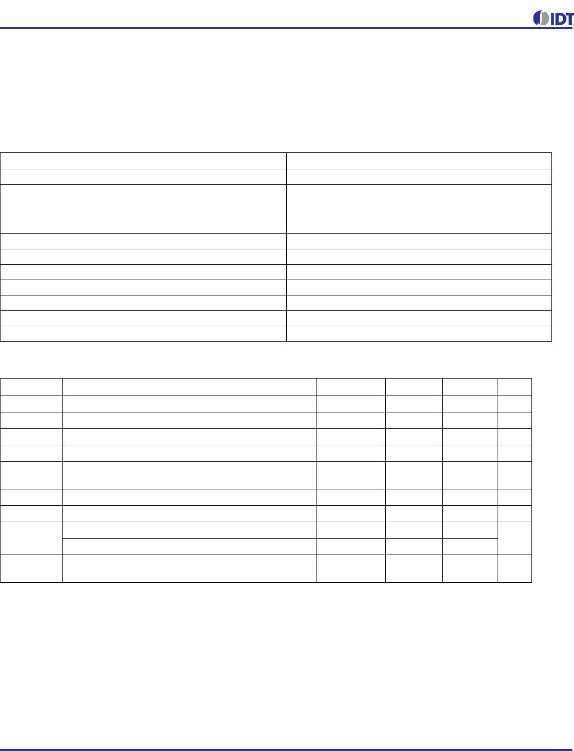
Table 9: Input Capacitance, LVCMOS Output Impedance, and Internal Pull-down
Resistance
(T
A
= +25 °C)
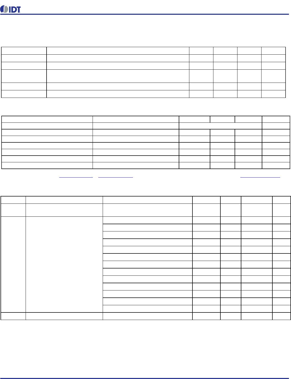
Table 10: Crystal Characteristics
Note: Typical crystal used is IDT 603-25-150 or FOX 603-25-150. For different reference crystal options please go to www.foxonline.com.
Table 11: DC Electrical Characteristics
1. Single CMOS driver active.
2. Measured into a 5” 50 Ohm trace with 2 pF load.
3. Iddcore = IddA + IddD, no loads.
Symbol Parameter Min Typ Max Unit
CIN
Input Capacitance (SD/OE, SEL1/SDA, SEL0/SCL)
37pF
Pull-down Resistor 100 300 k
ROUT
LVCMOS Output Driver Impedance (VDDO = 1.8V, 2.5V, 3.3V)
17
XIN/REF
Programmable capacitance at XIN/REF
925pF
XOUT
Programmable capacitance at XOUT
925pF
Parameter Test Conditions Minimum Typical Maximum Units
Mode of Oscillation
Frequency 82540MHz
Equivalent Series Resistance (ESR) 10 100
Shunt Capacitance 7pF
Load Capacitance (CL) @ <=25 MHz 6 8 12 pF
Load Capacitance (CL) >25M to 40M 6 8 pF
Maximum Crystal Drive Level 100 µW
Fundamental
Symbol Parameter Test Conditions Min Typ Max Unit
Iddcore
3
Core Supply Current
100 MHz on all outputs, 25 MHz
REFCLK
45mA
LVPECL, 350 MHz, 3.3V VDDOx 35 37 mA
LVPECL, 350 MHz, 2.5V VDDOx 33 35 mA
LVDS, 350 MHz, 3.3V VDDOx 8 9 mA
LVDS, 350 MHz, 2.5V VDDOx 7 8 mA
LVDS, 350 MHz, 1.8V VDDOx 6 7 mA
HCSL, 250 MHz, 3.3V VDDOx, 2 pF load 22 23 mA
HCSL, 250 MHz, 2.5V VDDOx, 2 pF load 20 22 mA
LVCMOS, 50 MHz, 3.3V, VDDOx
1,2
56mA
LVCMOS, 50 MHz, 2.5V, VDDOx
1,2
45mA
LVCMOS, 50 MHz, 1.8V, VDDOx
1,2
34mA
LVCMOS, 200 MHz, 3.3V VDDOx
1
17 18 mA
LVCMOS, 200 MHz, 2.5V VDDOx
1,2
12 13 mA
LVCMOS, 200 MHz, 1.8V VDDOx
1,2
910mA
Iddpd Power Down Current SD asserted, I2C Programming 5 6 mA
Iddox Output Buffer Supply Current
PROGRAMMABLE FANOUT BUFFER 12 REVISION D 07/13/15
5P1103 DATASHEET
Table 12: Electrical Characteristics – Differential Clock Input Parameters
1,2
(Supply
Voltage V
DDA
, V
DDD
, V
DDO
0
= 3.3V ±5%, 2.5V ±5%, 1.8V ±5%, TA = -40°C to +85°C)
1. Guaranteed by design and characterization, not 100% tested in production.
2. Slew rate measured through ±75mV window centered around differential zero.
Table 13: DC Electrical Characteristics for 3.3V LVCMOS (V
DDO
= 3.3V±5%, TA = -40°C to +85°C)
1
1. See “Recommended Operating Conditions” table.
Symbol Parameter Test Conditions Min Typ Max Unit
V
IH
Input HIGH Voltage–CLKIN, CLKINB Single-ended input 0.55 1.7 V
V
IL
Input LOW Voltage–CLKIN, CLKINB Single-ended input GND - 0.3 0.4 V
V
SWING
Input Amplitude - CLKIN, CLKINB Peak to Peak value, single-ended 200 1200 mV
dv/dt Input Slew Rate - CLKIN, CLKINB Measured differentially 0.4 8 V/ns
I
IL
Input Leakage Low Current V
IN
= GND -5 5 µA
I
IH
Input Leakage High Current V
IN
= 1.7V 20 µA
d
TIN
Input Duty Cycle Measurement from differential
waveform
45 55 %
Symbol Parameter Test Conditions Min Typ Max Unit
VOH Output HIGH Voltage
IOH = -15mA
2.4 VDDO V
VOL Output LOW Voltage
IOL = 15mA
0.4 V
IOZDD Output Leakage Current (OUT1~4)
Tri-state outputs, VDDO = 3.465V
A
IOZDD Output Leakage Current (OUT0)
Tri-state outputs, VDDO = 3.465V
30 µA
VIH Input HIGH Voltage
Single-ended inputs - CLKSEL, SD/OE
0.7xVDDD VDDD + 0.3 V
VIL Input LOW Voltage
Single-ended inputs - CLKSEL, SD/OE
GND - 0.3 0.3xVDDD V
VIH Input HIGH Voltage
Single-ended input OUT0_SEL_I2CB
2 VDDO0 + 0.3 V
VIL Input LOW Voltage
Single-ended input OUT0_SEL_I2CB
GND - 0.3 0.4 V
VIH Input HIGH Voltage
Single-ended input - XIN/REF
0.8 1.2 V
VIL Input LOW Voltage
Single-ended input - XIN/REF
GND - 0.3 0.4 V
T
R
/T
F
Input Rise/Fall Time
CLKSEL, SD/OE, SEL1/SDA,
SEL0/SCL
300 nS

5P1103A000NLGI

Mfr. #:
Manufacturer:
IDT
Description:
Clock Buffer 2 to 4 Output OTP 1.8 to 3.3V Prog Out
Lifecycle:
New from this manufacturer.
Delivery:
DHL FedEx Ups TNT EMS
Payment:
T/T Paypal Visa MoneyGram Western Union

Products related to this Datasheet