REVISION D 07/13/15 7 PROGRAMMABLE FANOUT BUFFER
5P1103 DATASHEET
its independent output power pin (V
DDO
) and thus each can
have different output voltage levels. Output voltage levels of
2.5V or 3.3V are supported for differential HCSL, LVPECL
operation, and 1. 8V, 2.5V, or 3.3V are supported for LVCMOS
and differential LVDS operation.
Each output may be enabled or disabled by register bits.
When disabled an output will be in a logic 0 state as
determined by the programming bit table shown on page 6.
LVCMOS Operation
When a given output is configured to provide LVCMOS levels,
then both the OUTx and OUTxB outputs will toggle at the
selected output frequency. All the previously described
configuration and control apply equally to both outputs.
Frequency, phase alignment, voltage levels and enable /
disable status apply to both the OUTx and OUTxB pins. The
OUTx and OUTxB outputs can be selected to be
phase-aligned with each other or inverted relative to one
another by register programming bits. Selection of
phase-alignment may have negative effects on the phase
noise performance of any part of the device due to increased
simultaneous switching noise within the device.
Device Hardware Configuration
The 5P1103 supports an internal One-Time Programmable
(OTP) memory that can be pre-programmed at the factory
with up to 4 complete device configuration.
These configurations can be over-written using the serial
interface once reset is complete. Any configuration written via
the programming interface needs to be re-written after any
power cycle or reset. Please contact IDT if a specific
factory-programmed configuration is desired.
Device Start-up & Reset Behavior
The 5P1103 has an internal power-up reset (POR) circuit. The
POR circuit will remain active for a maximum of 10ms after
device power-up.
Upon internal POR circuit expiring, the device will exit reset
and begin self-configuration.
The device will load internal registers using the configuration
stored in the internal One-Time Programmable (OTP)
memory.
Once the full configuration has been loaded, the device will
respond to accesses on the serial port and will attempt to
begin operation.
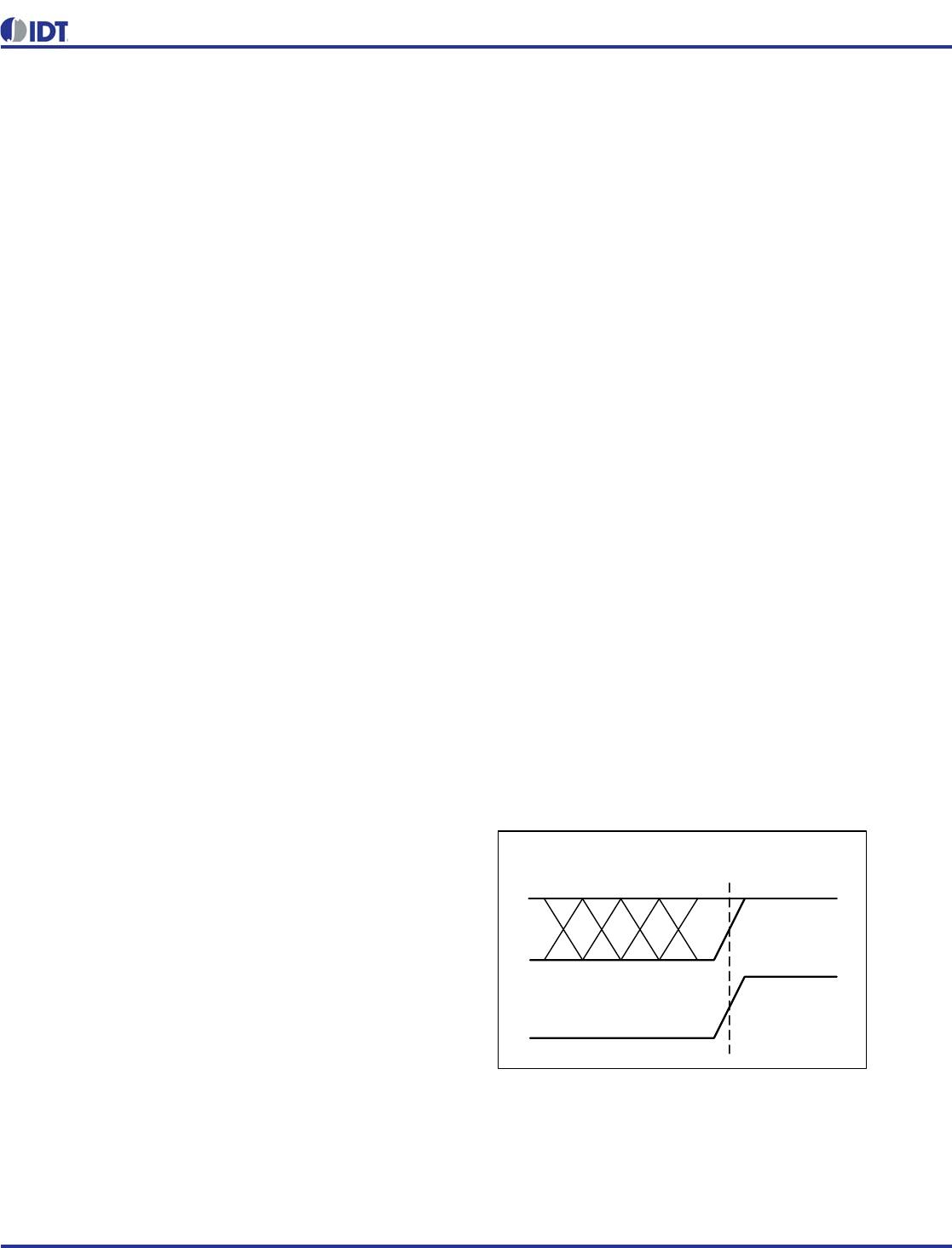
Power Up Ramp Sequence
VDDA and VDDD must ramp up together. VDDO0~2 must
ramp up before, or concurrently with, VDDA and VDDD. All
power supply pins must be connected to a power rail even if
the output is unused. All power supplies must ramp in a linear
fashion and ramp monotonically.
VDDO0~2
VDDA
VDDD
PROGRAMMABLE FANOUT BUFFER 8 REVISION D 07/13/15
5P1103 DATASHEET
I
2
C Mode Operation
The device acts as a slave device on the I
2
C bus using one of
the two I
2
C addresses (0xD0 or 0xD4) to allow multiple
devices to be used in the system. The interface accepts
byte-oriented block write and block read operations. Two
address bytes specify the register address of the byte position
of the first register to write or read. Data bytes (registers) are
accessed in sequential order from the lowest to the highest
byte (most significant bit first). Read and write block transfers
can be stopped after any complete byte transfer. During a
write operation, data will not be moved into the registers until
the STOP bit is received, at which point, all data received in
the block write will be written simultaneously.
For full electrical I
2
C compliance, it is recommended to use
external pull-up resistors for SDATA and SCLK. The internal
pull-down resistors have a size of 100k typical.
I
2
C Slave Read and Write Cycle Sequencing
REVISION D 07/13/15 9 PROGRAMMABLE FANOUT BUFFER
5P1103 DATASHEET
Table 5: I
2
C Bus DC Characteristics
Table 6: I
2
C Bus AC Characteristics
Note 1: A device must internally provide a hold time of at least 300 ns for the SDA signal (referred to the V
IH
(MIN) of the SCL signal) to bridge the undefined region of the falling edge
of SCL.
Note 2: I2C inputs are 5V tolerant.
Symbol Parameter Conditions Min Typ Max Unit
V
IH
Input HIGH Level For SEL1/SDA pin and
SEL0/SCL pin.
0.7xV
DDD
5.5
2
V
V
IL
Input LOW Level For SEL1/SDA pin and
SEL0/SCL pin.
GND-0.3 0.3xV
DDD
V
V
HYS
Hysteresis of Inputs 0.05xV
DDD
V
I
IN
Input Leakage Current -1 30 µA
V
OL
Output LOW Voltage I
OL
= 3 mA 0.4 V
Symbol Parameter Min Typ Max Unit
F
SCLK
Serial Clock Frequency (SCL) 10 400 kHz
t
BUF
Bus free time between STOP and START 1.3 µs
t
SU:START
Setup Time, START 0.6 µs
t
HD:START
Hold Time, START 0.6 µs
t
SU:DATA
Setup Time, data input (SDA) 100 ns
t
HD:DATA
Hold Time, data input (SDA)
1
s
t
OVD
Output data valid from clock 0.9 µs
C
B
Capacitive Load for Each Bus Line 400 pF
t
R
Rise Time, data and clock (SDA, SCL) 20 + 0.1xC
B
300 ns
t
F
Fall Time, data and clock (SDA, SCL) 20 + 0.1xC
B
300 ns
t
HIGH
HIGH Time, clock (SCL) 0.6 µs
t
LOW
LOW Time, clock (SCL) 1.3 µs
t
SU:STOP
Setup Time, STOP 0.6 µs

5P1103A000NLGI

Mfr. #:
Manufacturer:
IDT
Description:
Clock Buffer 2 to 4 Output OTP 1.8 to 3.3V Prog Out
Lifecycle:
New from this manufacturer.
Delivery:
DHL FedEx Ups TNT EMS
Payment:
T/T Paypal Visa MoneyGram Western Union

Products related to this Datasheet