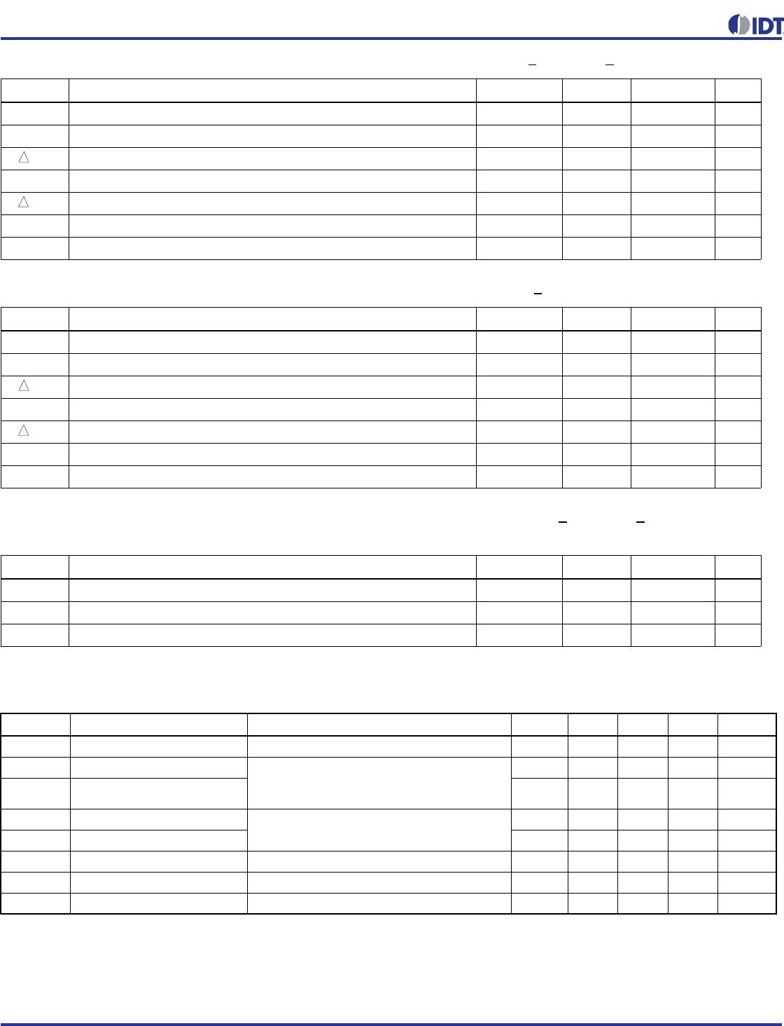
REVISION D 07/13/15 13 PROGRAMMABLE FANOUT BUFFER
5P1103 DATASHEET
Table 14: DC Electrical Characteristics for 2.5V LVCMOS (V
DDO
= 2.5V±5%, TA = -40°C to +85°C)
Table 15: DC Electrical Characteristics for 1.8V LVCMOS
(V
DDO
= 1.8V±5%, TA = -40°C to +85°C)
Symbol Parameter Test Conditions Min Typ Max Unit
VOH Output HIGH Voltage
IOH = -12mA
0.7xVDDO VDDD + 0.3 V
VOL Output LOW Voltage
IOL = 12mA
0.4 V
IOZDD Output Leakage Current
Tri-state outputs, VDDO = 2.625V
A
VOH Output HIGH Voltage
IOH = -12mA, OUT0
0.6 xVDDO VDDD + 0.3 V
VOL Output LOW Voltage
IOL = 12mA, OUT0
0.4 V
IOZDD Output Leakage Current
Tri-state outputs, VDDO = 2.625V, OUT0
30 µA
VIH Input HIGH Voltage
Single-ended inputs - CLKSEL, SD/OE
0.7xVDDD VDDD + 0.3 V
VIL Input LOW Voltage
Single-ended inputs - CLKSEL, SD/OE
GND - 0.3 0.3xVDDD V
VIH Input HIGH Voltage
Single-ended input OUT0_SEL_I2CB
1.7
VDDO0 + 0.3
5
V
VIL Input LOW Voltage
Single-ended input OUT0_SEL_I2CB
GND - 0.3 0.4 V
VIH Input HIGH Voltage
Single-ended input - XIN/REF
0.8 1.2 V
VIL Input LOW Voltage
Single-ended input - XIN/REF
GND - 0.3 0.4 V
T
R
/T
F
Input Rise/Fall Time
CLKSEL, SD/OE, SEL1/SDA,
SEL0/SCL
300 nS
Symbol Parameter Test Conditions Min Typ Max Unit
VOH Output HIGH Voltage
IOH = -8mA
0.7 xVDDO VDDO V
VOL Output LOW Voltage
IOL = 8mA
0.25 x VDDO V
IOZDD Output Leakage Current
Tri-state outputs, VDDO = 3.465V
A
VOH Output HIGH Voltage
IOH = -8mA, OUT0
0.6 xVDDO VDDO V
VOL Output LOW Voltage
IOL = 8mA, OUT0
0.25 x VDDO V
IOZDD Output Leakage Current
Tri-state outputs, VDDO = 3.465V, OUT0
30 µA
VIH Input HIGH Voltage
Single-ended inputs - CLKSEL, SD/OE
0.7 * VDDD VDDD + 0.3 V
VIL Input LOW Voltage
Single-ended inputs - CLKSEL, SD/OE
GND - 0.3 0.3 * VDDD V
VIH Input HIGH Voltage
Single-ended input OUT0_SEL_I2CB
0.65 * VDDO0 VDDD0 + 0.3 V
VIL Input LOW Voltage
Single-ended input OUT0_SEL_I2CB
GND - 0.3 0.4 V
VIH Input HIGH Voltage
Single-ended input - XIN/REF
0.8 1.2 V
VIL Input LOW Voltage
Single-ended input - XIN/REF
GND - 0.3 0.4 V
T
R
/T
F
Input Rise/Fall Time
CLKSEL, SD/OE, SEL1/SDA,
SEL0/SCL
300 nS
PROGRAMMABLE FANOUT BUFFER 14 REVISION D 07/13/15
5P1103 DATASHEET
Table 16: DC Electrical Characteristics for LVDS(V
DDO
= 3.3V+5% or 2.5V+5%, TA = -40°C to +85°C)
Table 17: DC Electrical Characteristics for LVDS (V
DDO
= 1.8V+5%, TA = -40°C to +85°C)
Table 18: DC Electrical Characteristics for LVPECL (V
DDO
= 3.3V+5% or 2.5V+5%, TA = -40°C to
+85°C)
Table 19: Electrical Characteristics – DIF 0.7V Low Power HCSL Differential Outputs
(V
DDO
= 3.3V±5%, 2.5V±5%, TA = -40°C to +85°C)
1. Guaranteed by design and characterization. Not 100% tested in production
2. Measured from differential waveform.
3. Slew rate is measured through the V
SWING
voltage range centered around differential 0V. This results in a +/-150mV window around differential 0V.
4. V
CROSS
is defined as voltage where Clock = Clock# measured on a component test board and only applies to the differential rising edge (i.e. Clock rising and Clock# falling).
5. The total variation of all V
CROSS
measurements in any particular system. Note that this is a subset of V
CROSS
min/max (V
CROSS
absolute) allowed. The intent is to limit V
CROSS
induced modulation by setting V
CROSS
to be smaller than V
CROSS
absolute.
6. Measured from single-ended waveform.
7. Measured with scope averaging off, using statistics function. Variation is difference between min. and max.
Symbol Parameter Min Typ Max Unit
V
OT
(+) Differential Output Voltage for the TRUE binary state 247 454 mV
V
OT
(-) Differential Output Voltage for the FALSE binary state -247 -454 mV
V
OT
Change in V
OT
between Complimentary Output States 50 mV
V
OS
Output Common Mode Voltage (Offset Voltage) 1.125 1.25 1.375 V
V
OS
Change in V
OS
between Complimentary Output States 50 mV
I
OS
Outputs Short Circuit Current, V
OUT
+ or V
OUT
- = 0V or V
DDO
924mA
I
OSD
Differential Outputs Short Circuit Current, V
OUT
+ = V
OUT
-612mA
Symbol Parameter Min Typ Max Unit
V
OT
(+) Differential Output Voltage for the TRUE binary state 247 454 mV
V
OT
(-) Differential Output Voltage for the FALSE binary state -247 -454 mV
V
OT
Change in V
OT
between Complimentary Output States 50 mV
V
OS
Output Common Mode Voltage (Offset Voltage) 0.8 0.875 0.95 V
V
OS
Change in V
OS
between Complimentary Output States 50 mV
I
OS
Outputs Short Circuit Current, V
OUT
+ or V
OUT
- = 0V or V
DDO
924mA
I
OSD
Differential Outputs Short Circuit Current, V
OUT
+ = V
OUT
-612mA
Symbol Parameter Min Typ Max Unit
V
OH
Output Voltage HIGH, terminated through 50 tied to V
DD
- 2 V V
DDO
- 1.19 V
DDO
- 0.69 V
V
OL
Output Voltage LOW, terminated through 50 tied to V
DD
- 2 V V
DDO
- 1.94 V
DDO
- 1.4 V
V
SWING
Peak-to-Peak Output Voltage Swing 0.55 0.993 V
Symbol Parameter Conditions Min Typ Max Units Notes
dV/dt Slew Rate Scope averaging on 1 4 V/ns 1,2,3
V
HIGH
Voltage High Statistical measurement on single-ended
signal using oscilloscope math function
(Scope averaging ON)
660 850 mV 1,6,7
V
LOW
Voltage Low -150 150 mV 1,6
V
MAX
Maximum Voltage Measurement on single-ended signal using
absolute value (Scope averaging off)
1150 mV 1
V
MIN
Minimum Voltage -300 mV 1
V
SWING
Voltage Swing Scope averaging off 300 mV 1,2,6
V
CROSS
Crossing Voltage Value Scope averaging off 250 550 mV 1,4,6
V
CROSS
Crossing Voltage Variation Scope averaging off 140 mV 1,5
REVISION D 07/13/15 15 PROGRAMMABLE FANOUT BUFFER
5P1103 DATASHEET
Table 20: AC Timing Electrical Characteristics
(V
DDO
= 3.3V+5% or 2.5V+5% or 1.8V ±5%, TA = -40°C to +85°C)
(Spread Spectrum Generation = OFF)
Symbol
Parameter Test Conditions
Min. Typ. Max. Units
Input frequency limit (XIN)
840MHz
Input frequency limit (REF)
1200MHz
Input frequency limit (CLKIN, CLKINB)
1350MHz
Single ended clock output limit (LVCMOS)
1200
Differential cock output limit (LVPECL/ LVDS/HCSL)
1350
t2 Input Duty Cycle
Duty Cycle
45 50 55 %
LVPECL Output Duty Cycle Distortion -5 5 %
HCSL Output Duty Cycle Distortion -5 5 %
LVCMOS Output Duty Cycle Distortion @ 2.5V and 3.3V -5 5 %
LVCMOS Output Duty Cycle Distortion @ 1.8 V, f <100MHz -5 5 %
LVCMOS Output Duty Cycle Distortion @ 1.8 V, f >=100MHz -10 10 %
Slew Rate, SLEW[1:0] = 11
Single-ended 3.3V LVCMOS output clock rise and fall time, @ 125MHz
25% to 75% of VDDO (Output Load = 5 pF)
1.7 2.7 4.1 V/ns
Slew Rate, SLEW[1:0] = 10
Single-ended 3.3V LVCMOS output clock rise and fall time, @ 125MHz
25% to 75% of VDDO (Output Load = 5 pF)
1.4 2.4 3.8 V/ns
Slew Rate, SLEW[1:0] = 01
Single-ended 3.3V LVCMOS output clock rise and fall time, @ 125MHz
25% to 75% of VDDO (Output Load = 5 pF)
1.3 2.3 3.7 V/ns
Slew Rate, SLEW[1:0] = 00
Single-ended 3.3V LVCMOS output clock rise and fall time, @ 125MHz
25% to 75% of VDDO (Output Load = 5 pF)
1.1 2.1 3.6 V/ns
Slew Rate, SLEW[1:0] = 11
Single-ended 2.5V LVCMOS output clock rise and fall time, @ 125MHz
25% to 75% of VDDO (Output Load = 5 pF)
0.9 1.7 2.6 V/ns
Slew Rate, SLEW[1:0] = 10
Single-ended 2.5V LVCMOS output clock rise and fall time, @ 125MHz
25% to 75% of VDDO (Output Load = 5 pF)
0.6 1.4 2.3 V/ns
Slew Rate, SLEW[1:0] = 01
Single-ended 2.5V LVCMOS output clock rise and fall time, @ 125MHz
25% to 75% of VDDO (Output Load = 5 pF)
0.6 1.3 2.2 V/ns
Slew Rate, SLEW[1:0] = 00
Single-ended 2.5V LVCMOS output clock rise and fall time, @ 125MHz
25% to 75% of VDDO (Output Load = 5 pF)
0.6 1.2 2.1 V/ns
Slew Rate, SLEW[1:0] = 11
Single-ended 1.8V LVCMOS output clock rise and fall time, @ 125MHz
25% to 75% of VDDO (Output Load = 5 pF)
0.7 1.2 2.1 V/ns
Slew Rate, SLEW[1:0] = 10
Single-ended 1.8V LVCMOS output clock rise and fall time, @ 125MHz
25% to 75% of VDDO (Output Load = 5 pF)
0.4 0.9 1.7 V/ns
Slew Rate, SLEW[1:0] = 01
Single-ended 1.8V LVCMOS output clock rise and fall time, @ 125MHz
25% to 75% of VDDO (Output Load = 5 pF)
0.4 0.8 1.6 V/ns
Slew Rate, SLEW[1:0] = 00
Single-ended 1.8V LVCMOS output clock rise and fall time, @ 125MHz
25% to 75% of VDDO (Output Load = 5 pF)
0.3 0.7 1.4 V/ns
Rise Times
LVDS, 20% to 80%, single-ended
300
Fall Times
LVDS, 80% to 20%, single-ended
300
Rise Times
LVPECL, 20% to 80%, single-ended
400
Fall Times
LVPECL, 80% to 20%, single-ended
400
t6
Buffer Additive Phase Jitter, RM
S
fREF=125MHz, LVCMOS, Vpp=1V, Integration range: 12kHz–20MHz
0.2 ps
t7 Output Skew
Skew between the same frequencies, with outputs using the same driver
format and phase delay set to 0 ns.
35 ps
Input to Output Skew Skew from input to output
3ns
t4
t5 ps
fIN Input Frequency
fOUT MHzOutput Frequency
t3 Output Duty Cycle Distortion

5P1103A000NLGI

Mfr. #:
Manufacturer:
IDT
Description:
Clock Buffer 2 to 4 Output OTP 1.8 to 3.3V Prog Out
Lifecycle:
New from this manufacturer.
Delivery:
DHL FedEx Ups TNT EMS
Payment:
T/T Paypal Visa MoneyGram Western Union

Products related to this Datasheet