Expand menu
Hello, Sign in
My Account
0
Cart
Home
Products
Sensors
Semiconductors
Passive Components
Connectors
Power
Electromechanical
Optoelectronics
Circuit Protection
Integrated Circuits - ICs
Main Products
Manufacturers
Blog
Services
About OMO
About Us
Contact Us
Check Stock
5P1103A000NLGI
P1-P3
P4-P6
P7-P9
P10-P12
P13-P15
P16-P18
P19-P21
P22-P24
P25-P27
P28-P30
P31-P32
PROGRAMMABLE FANOUT BUFFER
28
REVISION D 07/13/15
5P1103 DATASHEET
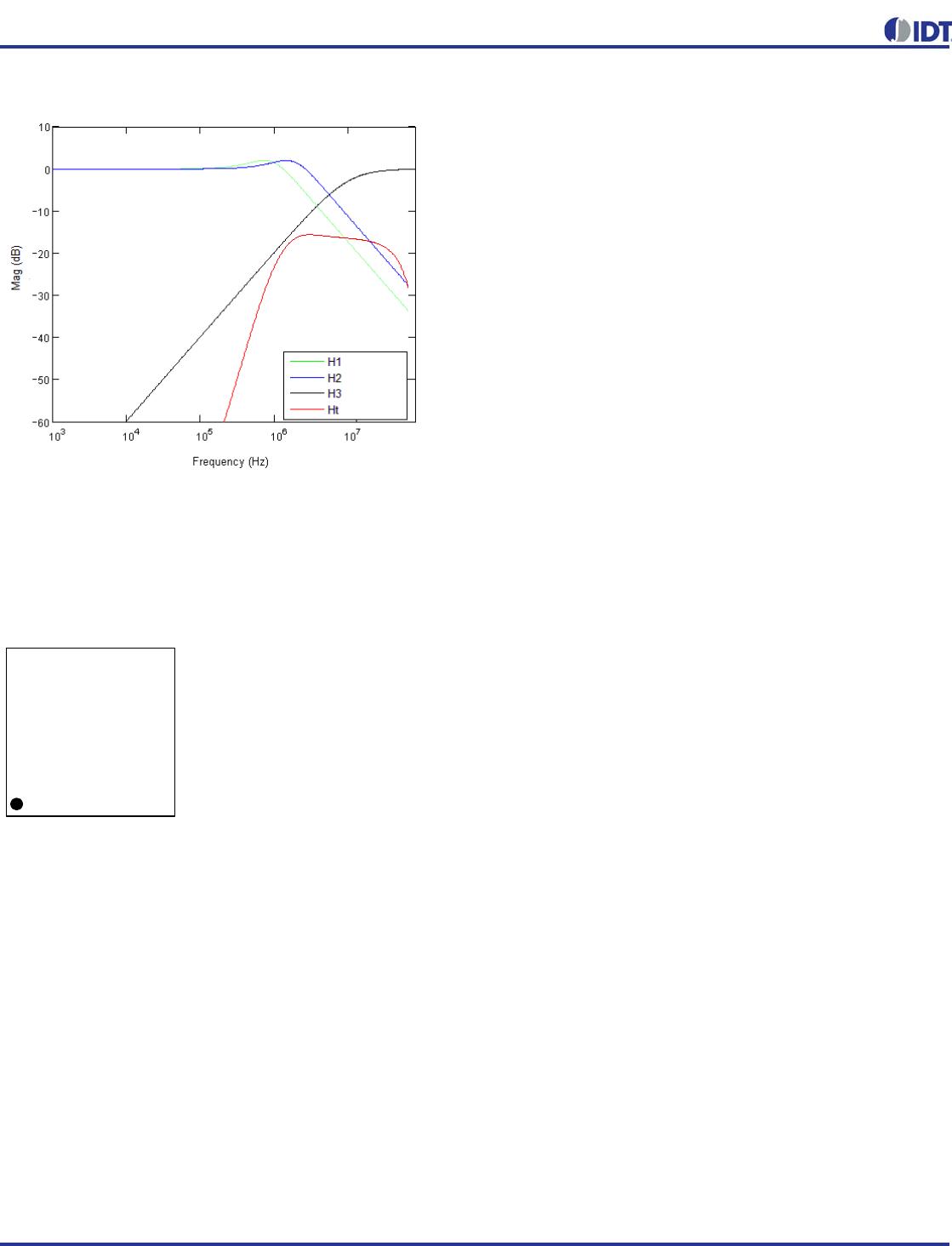
PCIe Gen3 Magnitude of T
ransfer Function
For a more thorough overvie
w of PCI Express jitter analysis
methodology
, please refer to IDT Application Note PCI
Express Reference Cl
ock R
equirements.
Marking Diagram
1. Line 1 is the truncated part number
.
2. “ddd” denotes da
sh code.
3. “YWW” is the last dig
it of the year
and week that the part was asse
mbled.
4. “
**
” denotes sequential l
ot number
.
5. “$” denotes mark code.
1103A
ddd
YWW**$
REVISION D 07/13/15
29
PROGRAMMABLE FANOUT BUFFER
5P1103 DATASHEET
Package Outline and Package Dimensions
(24-pin 4mm x 4mm VFQFPN)
www.IDT.com
T
I
D
PROGRAMMABLE FANOUT BUFFER
30
REVISION D 07/13/15
5P1103 DATASHEET
Package Outline and Pack
age Dimensions, cont.
(24-pin 4mm x 4mm VFQFPN)
www.IDT.com
T
I
D
P1-P3
P4-P6
P7-P9
P10-P12
P13-P15
P16-P18
P19-P21
P22-P24
P25-P27
P28-P30
P31-P32
5P1103A000NLGI
Mfr. #:
Buy 5P1103A000NLGI
Manufacturer:
IDT
Description:
Clock Buffer 2 to 4 Output OTP 1.8 to 3.3V Prog Out
Lifecycle:
New from this manufacturer.
Delivery:
DHL
FedEx
Ups
TNT
EMS
Payment:
T/T
Paypal
Visa
MoneyGram
Western
Union
Products related to this Datasheet
5P1103A000NLGI
5P1103A512NLGI