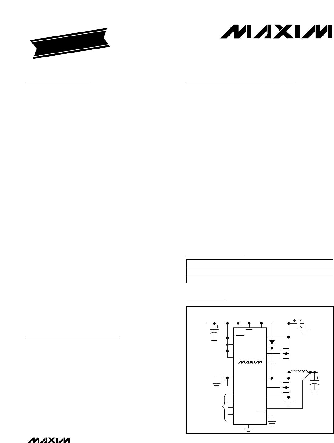
MAX1710/MAX1711/MAX1712
High-Speed, Digitally Adjusted
Step-Down Controllers for Notebook CPUs
2 _______________________________________________________________________________________
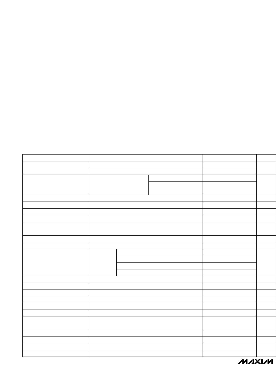
ABSOLUTE MAXIMUM RATINGS
Stresses beyond those listed under “Absolute Maximum Ratings” may cause permanent damage to the device. These are stress ratings only, and functional
operation of the device at these or any other conditions beyond those indicated in the operational sections of the specifications is not implied. Exposure to
absolute maximum rating conditions for extended periods may affect device reliability.
V+ to GND ..............................................................-0.3V to +30V
V
CC
, V
DD
to GND .....................................................-0.3V to +6V
PGND to GND.....................................................................±0.3V
SHDN, PGOOD to GND ...........................................-0.3V to +6V
OVP, ILIM, FB, FBS, CC, REF, D0–D4,
GNDS, TON to GND..............................-0.3V to (V
CC
+ 0.3V)
SKIP to GND (Note 1).................................-0.3V to (V
CC
+ 0.3V)
DL to PGND................................................-0.3V to (V
DD
+ 0.3V)
BST to GND ............................................................-0.3V to +36V
DH to LX .....................................................-0.3V to (BST + 0.3V)
LX to BST..................................................................-6V to +0.3V
REF Short Circuit to GND ...........................................Continuous
Continuous Power Dissipation (T
A
= +70°C)
24-Pin QSOP (derate 9.5mW/°C above +70°C)..........762mW
Operating Temperature Range ...........................-40°C to +85°C
Junction Temperature......................................................+150°C
Storage Temperature Range .............................-65°C to +165°C
Lead Temperature (soldering, 10s) .................................+300°C
V
BATT
= 4.5V to 28V, includes
load regulation error
SHDN = 0, measured at V+ = 28V, V
CC
= V
DD
= 0 or 5V
SHDN = 0
V
CC,
V
DD
SHDN = 0
Battery voltage, V+
Measured at V+
Measured at V
DD
, FB forced above the regulation point
Measured at V
CC
, FB forced above the regulation point
Rising edge of SHDN to full I
LIM
(Note 2)
V
BATT
= 24V,
FB = 2V
(Note 2)
FB (MAX1710 only) or FBS
FB - FBS or GNDS - GND = 0 to 25mV
V
CC
= 4.5V to 5.5V, V
BATT
= 4.5V to 28V
CONDITIONS
µA<1 5
Shutdown Battery Supply
Current
µA<1 5Shutdown Supply Current (V
DD
)
µA<1 5Shutdown Supply Current (V
CC
)
µA25 40Quiescent Battery Supply Current
µA<1 5Quiescent Supply Current (V
DD
)
µA600 950Quiescent Supply Current (V
CC
)
ns400 500Minimum Off-Time
380 425 470
260 290 320
175 200 225
%
-1 1
DC Output Voltage Accuracy
TON = REF (400kHz)
4.5 5.5
V
228
Input Voltage Range
TON = GND (550kHz)
ns
140 160 180
On-Time
ms1.7Soft-Start Ramp Time
µA-1 1GNDS Input Bias Current
µA-0.2 0.2FB Input Bias Current
TON = open (300kHz)
mV3Remote-Sense Voltage Error
mV5Line Regulation Error
UNITMIN TYP MAXPARAMETER
Falling edge, hysteresis = 40mV
REF in regulation
I
REF
= 0 to 50µA
V
CC
= 4.5V to 5.5V, no external REF load
V1.6REF Fault Lockout Voltage
µA10REF Sink Current
V0.01Reference Load Regulation
V1.98 2 2.02Reference Voltage
TON = V
CC
(200kHz)
Note 1: SKIP may be forced below -0.3V, temporarily exceeding the absolute maximum rating, for the purpose of debugging proto-
type breadboards using the no-fault test mode. Limit the current drawn to -5mA maximum.
ELECTRICAL CHARACTERISTICS
(Circuit of Figure 1, V
BATT
= 15V, V
CC
= V
DD
= 5V, SKIP = GND, T
A
= 0°C to +85°C, unless otherwise noted.)
kΩ130 180 240
FB Input Resistance
(MAX1711/MAX1712)
DAC codes from 1.3V to 2V
-1.2 1.2
I
LOAD
= 0 to 7A mV9Load Regulation Error
DAC codes from 0.925V
to 1.275V