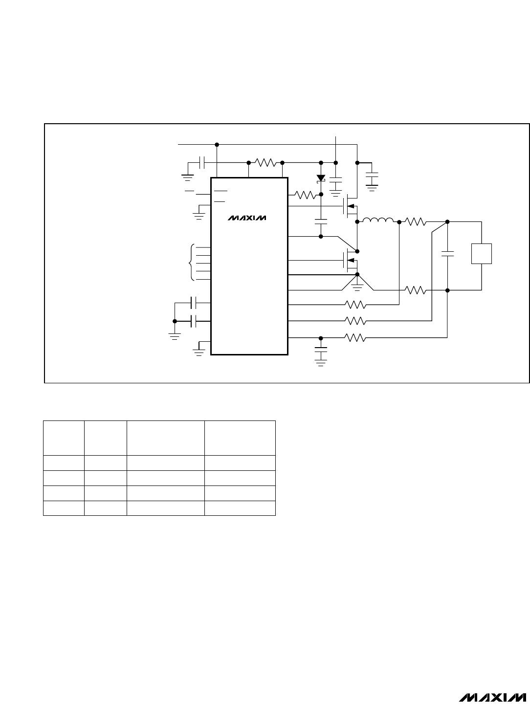
MAX1710/MAX1711/MAX1712
High-Speed, Digitally Adjusted
Step-Down Controllers for Notebook CPUs
______________________________________________________________________________________ 19
The actual microfarad capacitance value required relates
to the physical size needed to achieve low ESR, as well
as to the chemistry of the capacitor technology. Thus, the
capacitor is usually selected by ESR and voltage rating
rather than by capacitance value (this is true of tantalums,
OS-CONs, and other electrolytics).
When using low-capacity filter capacitors such as ceram-
ic or polymer types, capacitor size is usually determined
by the capacity needed to prevent the overvoltage pro-
tection circuit from being tripped when transitioning from
a full-load to a no-load condition. The capacitor must be
large enough to prevent the inductor’s stored energy from
launching the output above the overvoltage protection
threshold. Generally, once enough capacitance is added
to meet the overshoot requirement, undershoot at the ris-
ing load edge is no longer a problem (see also V
SAG
equation under Design Procedure).
With integrators disabled, the amount of overshoot due to
stored inductor energy can be calculated as:
where I
PEAK
is the peak inductor current. To absolutely
minimize the overshoot, disable the integrator first, since
the inherent delay of the integrator can cause extra “run-
on” switching cycles to occur after the load change.
Output Capacitor Stability Considerations
Stability is determined by the value of the ESR zero rela-
tive to the switching frequency. The point of instability is
given by the following equation:
For a typical 300kHz application, the ESR zero frequency
must be well below 95kHz, preferably below 50kHz.
Tantalum and OS-CON capacitors in widespread use at
the time of publication have typical ESR zero frequencies
of 15kHz. In the design example used for inductor selec-
tion, the ESR needed to support 50mVp-p ripple is
50mV/3.5A = 14.2mΩ. Three 470µF/4V Kemet T510 low-
ESR tantalum capacitors in parallel provide 15mΩ max
ESR. Their typical combined ESR results in a zero at
14.1kHz, well within the bounds of stability.
Don’t put high-value ceramic capacitors directly across
the fast feedback inputs (FB to GND) without taking pre-
cautions to ensure stability. Large ceramic capacitors
can have a high ESR zero frequency and cause erratic,
unstable operation. However, it’s easy to add enough
series resistance by placing the capacitors a couple of
inches downstream from the junction of the inductor and
FB pin (see the All-Ceramic-Capacitor Application sec-
tion).
Unstable operation manifests itself in two related but dis-
tinctly different ways: double-pulsing and fast-feedback
loop instability.
Double-pulsing occurs due to noise on FB or because
the ESR is so low that there isn’t enough voltage ramp in
the output voltage (FB) signal. This “fools” the error com-
parator into triggering a new cycle immediately after the
400ns minimum off-time period has expired. Double-
pulsing is more annoying than harmful, resulting in noth-
ing worse than increased output ripple. However, it can
indicate the possible presence of loop instability, which
is caused by insufficient ESR.
Loop instability can result in oscillations at the output
after line or load perturbations that can trip the overvolt-
age protection latch or cause the output voltage to fall
below the tolerance limit.
The easiest method for checking stability is to apply a
very fast zero-to-max load transient (see MAX1710
Evaluation Kit manual) and carefully observe the output
voltage ripple envelope for overshoot and ringing. It
can help to simultaneously monitor the inductor current
with an AC current probe. Don’t allow more than one
cycle of ringing after the initial step-response under- or
overshoot.
Input Capacitor Selection
The input capacitor must meet the ripple current
requirement (I
RMS
) imposed by the switching currents.
Nontantalum chemistries (ceramic, aluminum, or OS-
CON) are preferred due to their resistance to power-up
surge currents:
Power MOSFET Selection
Most of the following MOSFET guidelines focus on the
challenge of obtaining high load-current capability (>5A)
when using high-voltage (>20V) AC adapters. Low-cur-
rent applications usually require less attention.
For maximum efficiency, choose a high-side MOSFET
(Q1) that has conduction losses equal to the switching
losses at the optimum battery voltage (15V). Check to
ensure that the conduction losses at minimum input volt-
age don’t exceed the package thermal limits or violate
the overall thermal budget. Check to ensure that con-
duction losses plus switching losses at the maximum