MAX1710/MAX1711/MAX1712
High-Speed, Digitally Adjusted
Step-Down Controllers for Notebook CPUs
minimize the energy transferred from inductor to capaci-
tor during load-step recovery. Even so, the amount of
overshoot is high enough (80mV) that for the MAX1710,
it’s wise to disable OVP or use the MAX1711/MAX1712
with their fixed 2.25V overvoltage protection threshold to
avoid tripping the fault latch (see the overshoot equation
in the Output Capacitor Selection section). The efficiency
penalty for operating at 550kHz is about 2% to 3%,
depending on the input voltage.
Two optional 1k resistors are placed in series with FB
and FBS. These resistors prevent the negative output
voltage spike (that results from tripping OVP) from
pulling SHDN low via its internal ESD diode, which tends
to clear the fault latch, causing “hiccup” restarts.
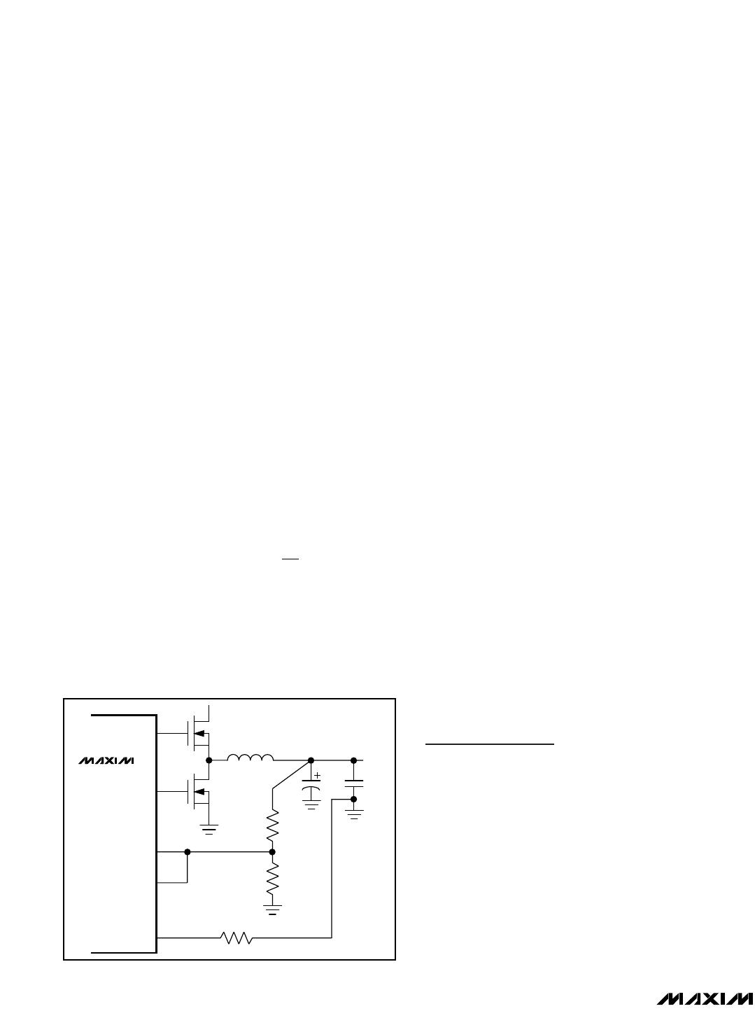
Setting V
OUT
with a Resistor-Divider
The output voltage can be adjusted with a resistor-
divider rather than the DAC if desired (Figure 8). The
drawback of this practice is that the on-time doesn’t
automatically receive correct compensation for changing
output voltage levels. This can result in variable switch-
ing frequency as the resistor ratio is changed and/or
excessive switching frequency. The equation for adjust-
ing the output voltage is:
where V
FB
is the currently selected DAC value. When
using external resistors, FBS remote sensing is not rec-
ommended, but GNDS remote sensing is still possible.
Connect FBS to FB and GNDS to remote ground loca-
tion. In resistor-adjusted circuits, the DAC code should
be set as close as possible to the actual output voltage
so that the switching frequency doesn’t become exces-
sive. For highest accuracy, use the MAX1710 when
adjusting V
OUT
with external resistors. The MAX1710 FB
node has very high impedance, while the MAX1711/
MAX1712 have a 180k ±35% FB impedance, which
degrades V
OUT
accuracy.
Adjusting V
OUT
Above 2V
The feed-forward circuit that makes the on-time depen-
dent on battery voltage maintains a nearly constant
switching frequency as V
IN
, I
LOAD
, and the DAC code
are changed. This works extremely well as long as FB is
connected directly to the output.
When the output is adjusted higher than 2V with a resis-
tor-divider, the switching frequency can be increased to
relatively unreasonable levels as the actual off-time
decreases and isn’t compensated for by a change in on-
time; 3.3V is about the maximum limit to the practical
adjustment range. Even at the slowest TON setting and
with the DAC set to 2V, the switching rate will exceed
600kHz.
The trip threshold for output overvoltage protection
scales with the nominal output voltage setting.
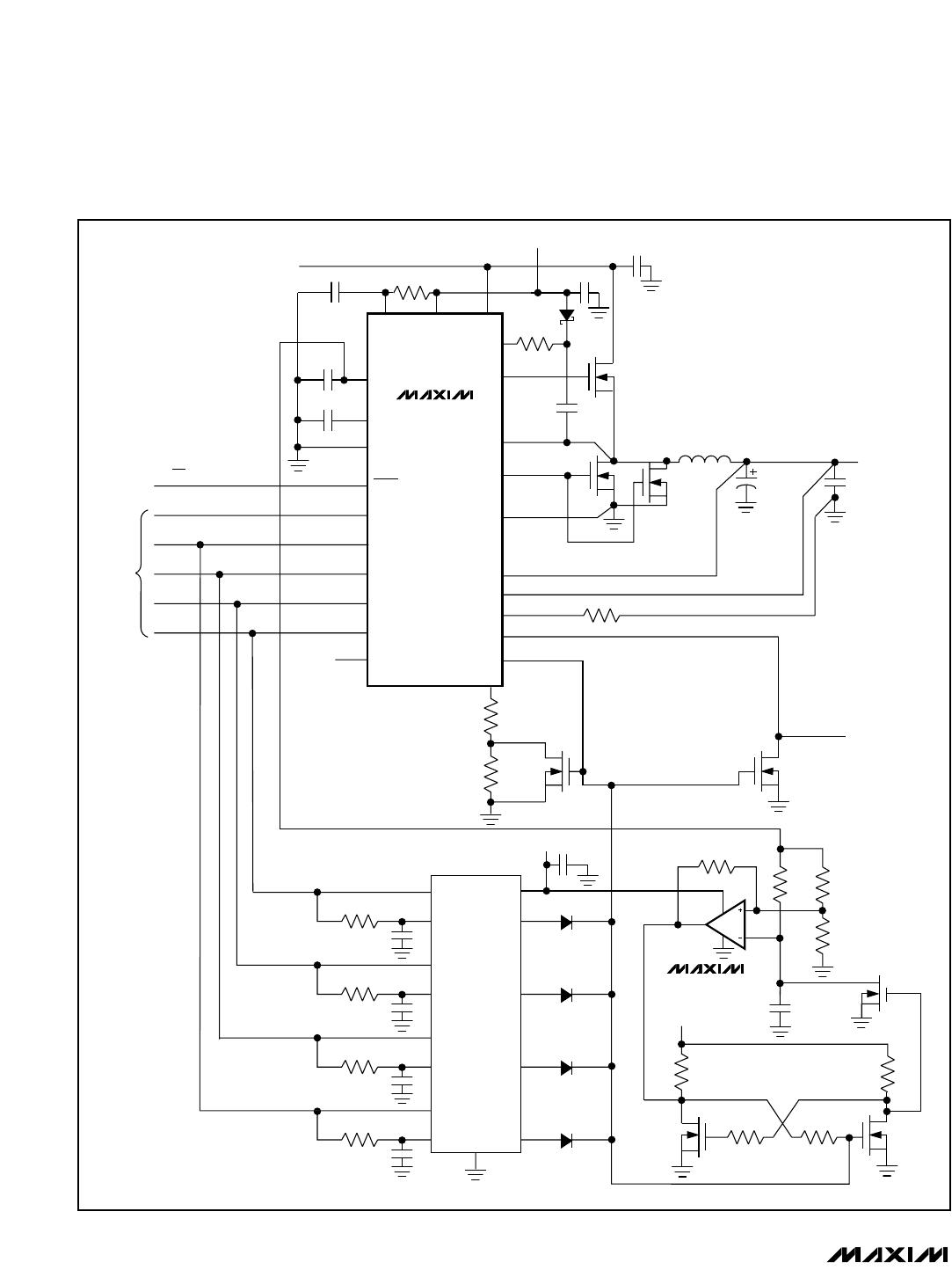
2-Stage (5V-Powered) Notebook CPU
Buck Regulator
The most efficient and overall cost-effective solution for
stepping down a high-voltage battery to very low output
voltage is to use a single-stage buck regulator that’s
powered directly from the battery. However, there may
be situations where the battery bus can’t be routed near
the CPU, or where space constraints dictate the smallest
possible local DC-DC converter. In such cases, the 5V-
powered circuit of Figure 9 may be appropriate. The
reduced input voltage allows a higher switching frequen-
cy and a much smaller inductor value.
Dynamic DAC Code Changes
(MAX1711/MAX1712)
Changing the output voltage dynamically by switching
DAC codes “on-the-fly” can be used to help make
power-savings/performance trade-offs in the host sys-
tem. Several important design issues arise from this
practice.
First, know that attempting to slew the output upward
quickly causes large current surges at the battery as the
IC goes into output current limiting during the transition.
Surge currents can be controlled either by counting the
DAC code slowly (50kHz or slower rate suggested), or
by modulating the I
LIM
current-limit threshold.
The DAC inputs must be driven quickly to the new value
so the device doesn’t wrongly interpret a disallowed
VV
R
R
OUT FB
=−
()
+
% 11
1
2
DL
DH
FB
FBS
GNDS
V
BATT
V
OUT
R1
1k
R2
MAX1710
MAX1711
MAX1712
Figure 8. Setting V
OUT
with a Resistor-Divider
22 ______________________________________________________________________________________
MAX1710/MAX1711/MAX1712
High-Speed, Digitally Adjusted
Step-Down Controllers for Notebook CPUs
______________________________________________________________________________________ 23
DAC code from the transitory value. Use 100ns maxi-
mum rise and fall times.
Selecting the output capacitors in dynamically adjusted
V
CORE
applications can be tricky due to trade-offs
between capacitor capacity and ESR. In other words, if
the capacitor has sufficiently low ESR to meet the load-
transient response specification, its large capacity may
cause excessive input surge currents. On the other
hand, a purely ceramic capacitor may not have enough
capacity to prevent overvoltage during the transition from
full- to no-load condition (see the overshoot equation
under Output Capacitor Selection). It may be necessary
to mix capacitor types or use specialized capacitors
such as those shown in Figure 7 in order to achieve the
required ESR while staying within the min/max capaci-
tance value window.
If the minimum load is very light, it may be necessary to
assert forced PWM mode (via SKIP) during the transition
period to guarantee some output sink current capability.
Otherwise, the output voltage won’t ramp downwards
until pulled down by external load current.
Using forced PWM mode repeatedly to ensure sink cur-
rent capability can have side effects, however. The ener-
gy taken from the output by the synchronous rectifier
isn’t lost, but is instead returned to the input. If the fre-
quency of the high-to-low output voltage transition is high
enough, efficiency will be degraded by the resistive “fric-
tion” losses associated with shuttling energy between
input and output capacitors. Also, if the output is being
overdriven by an external source (such as an external
docking-station power supply), forced PWM mode may
cause the battery voltage to become pumped up, possi-
bly overvoltaging the battery.
High-Power, Dynamically
Adjustable CPU Application
The MAX1711/MAX1712 V
CORE
regulator of Figure 10 is
designed to have its output voltage switched between
1.3V and 1.45V in less than 100µs, while causing a mini-
mum level of input surge current. To this end, the output
capacitors were selected for having the correct value to
a) support the needed ESR, b) prevent excess load-
I
LIM
V
CC
V
IN
4.5V TO 5.5V
TO REMOTE
LOAD
L1
0.5µH
V
OUT
1.6V AT 7A
SHDN
1µF
0.1µF
0.22µF
470pF
C2
3 x 470µF
KEMET
T510
IRF7805
IRF7805
1µF20
C1
4 x 10µF/25V
D0
D1
D2
D/A
INPUTS
ON/OFF
DL
LX
BST
DH
PGND
FB
1k
1k
GND
GNDS
FBS
V
DD
V
CC
V+
MAX1710
MAX1711
MAX1712
D4**
D3
REF
CC
TON
SKIP OVP*
100k
PGOOD
*MAX1710 ONLY
**MAX1711 ONLY
Figure 9. 5V-Powered, 7A CPU Buck Regulator
MAX1710/MAX1711/MAX1712
High-Speed, Digitally Adjusted
Step-Down Controllers for Notebook CPUs
IRF7805
OUTPUT
+1.5V AT 15A
10x
220µF
4V
OS-CON
2 x IRF7805
CMPSH3
6 x 10µF/25V CERAMIC
0.1µF
1µH/20A
1k
2
7
1
5
4
10
9
13
12
+3.3V
3M
1N4148
1N4148
1N4148
TRANSITION DETECTOR
1N4148
100k
1%
100k
1%
820pF
5%+3.3V
30k
100k 100k
2N7002
2N7002
POWERGOOD
2N7002
40k
1%
200k
1%
2N7002
TIMER BLOCK
2N7002
30k
49.9k
1%
0.1µF
REF
CC
GND
SHDN
D0
D1
D2
D3
D4
TON
N.C.
5
9
10
2
20
19
18
17
16
8
6
21
12
11
1k
4
3
14
13
23
24
22
1157
+5V INPUT
V
BATT
10V TO 22V
I
LIM
SKIP
PGOOD
GNDS
FBS
FB
PGND
DL
LX
DH
BST
V
CC
V
DD
V+
0.22µF
0.1µF
1µF
2
20µF
CERAMIC
20
470pF
1000pF
1k
1000pF
1k
1000pF
1k
1000pF
GND
B1
A1
B2
A2
B3
A3
B4
A4
3
6
8
11
14
Y1
Y2
Y3
Y4
V
CC
MAX1711
MAX1712
MAX986
74HC86
ON/OFF
LSB
MSB
DAC
INPUTS
Figure 10.15A Dynamically Adjustable Notebook CPU Supply with Battery-Surge Current Limiting
24 ______________________________________________________________________________________

MAX1712EEG

Mfr. #:
Manufacturer:
Maxim Integrated
Description:
LDO Voltage Controllers High-Speed, Digitally Adjusted Step-Down Controllers for Notebook CPUs
Lifecycle:
New from this manufacturer.
Delivery:
DHL FedEx Ups TNT EMS
Payment:
T/T Paypal Visa MoneyGram Western Union

Products related to this Datasheet