• Keep the high-current paths short, especially at the
ground terminals. This practice is essential for stable,
jitter-free operation.
• Connect GND and PGND together close to the IC.
Carefully follow the grounding instructions under step
4 of the Layout Procedure.
• Keep the power traces and load connections short.
This practice is essential for high efficiency. The use
of thick copper PC boards (2 oz vs. 1 oz) can en-
hance full-load efficiency by 1% or more. Correctly
routing PC board traces is a difficult task that must be
approached in terms of fractions of centimeters,
where a single milliohm of excess trace resistance
causes a measurable efficiency penalty.
• LX and PGND connections to Q2 for current limiting
must be made using Kelvin sense connections in
order to guarantee the current-limit accuracy. With
SO-8 MOSFETs, this is best done by routing power to
the MOSFETs from outside using the top copper
layer, while tying in PGND and LX inside (underneath)
the SO-8 package.
• When trade-offs in trace lengths must be made, it’s
preferable to allow the inductor charging path to be
made longer than the discharge path. For example,
it’s better to allow some extra distance between the
input capacitors and the high-side MOSFET than to
allow distance between the inductor and the low-side
MOSFET or between the inductor and the output filter
capacitor.
• Ensure that the FB connection to C
OUT
is short and
direct. However, in some cases it may be desirable to
deliberately introduce some trace length between the
FB inductor node and the output filter capacitor (see
the All-Ceramic-Capacitor Application section).
• Route high-speed switching nodes away from sensi-
tive analog areas (CC, REF, ILIM).
• Make all pin-strap control input connections (SKIP,
ILIM, etc.) to GND or V
CC
rather than PGND or V
DD
.
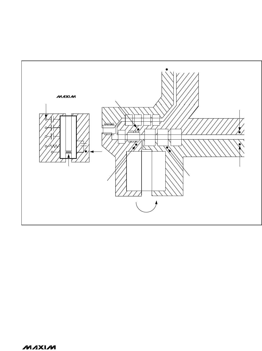
Layout Procedure
1) Place the power components first, with ground termi-
nals adjacent (Q2 source, CIN-, COUT-, D1 anode). If
possible, make all these connections on the top layer
with wide, copper-filled areas.
2) Mount the controller IC adjacent to MOSFET Q2,
preferably on the back side opposite Q2 to keep LX-
PGND current-sense lines and the DL gate-drive line
short and wide. The DL gate trace must be short and
wide, measuring 10 to 20 squares (50 to 100 mils
wide if the MOSFET is 1 inch from the controller IC).
3) Group the gate-drive components (BST diode and
capacitor, V
DD
bypass capacitor) together near the
controller IC.
4) Make the DC-DC controller ground connections as
shown in Figure 11. This diagram can be viewed as
having three separate ground planes: output ground,
where all the high-power components go; the PGND
plane, where the PGND pin and V
DD
bypass capaci-
tor go; and an analog GND plane, where sensitive
analog components go. The analog ground plane
and PGND plane must meet only at a single point
directly beneath the IC. These two planes are then
connected to the high-power output ground with a
short connection from V
DD
cap/PGND to the source
of the low-side MOSFET, Q2 (the middle of the star
ground). This point must also be very close to the out-
put capacitor ground terminal.
5) Connect the output power planes (V
CORE
and system
ground planes) directly to the output filter capacitor
positive and negative terminals with multiple vias.
Place the entire DC-DC converter circuit as close to
the CPU as is practical.
MAX1710/MAX1711/MAX1712
High-Speed, Digitally Adjusted
Step-Down Controllers for Notebook CPUs
26 ______________________________________________________________________________________