10µs/div
LOAD-TRANSIENT RESPONSE
(WITH INTEGRATOR)
V
IN
= 15V, V
O
= 1.6V, I
O
= 0A TO 7A
A = V
OUT
, AC-COUPLED, 50mV/div
B = INDUCTOR CURRENT, 5A/div
A
B
MAX1710-16
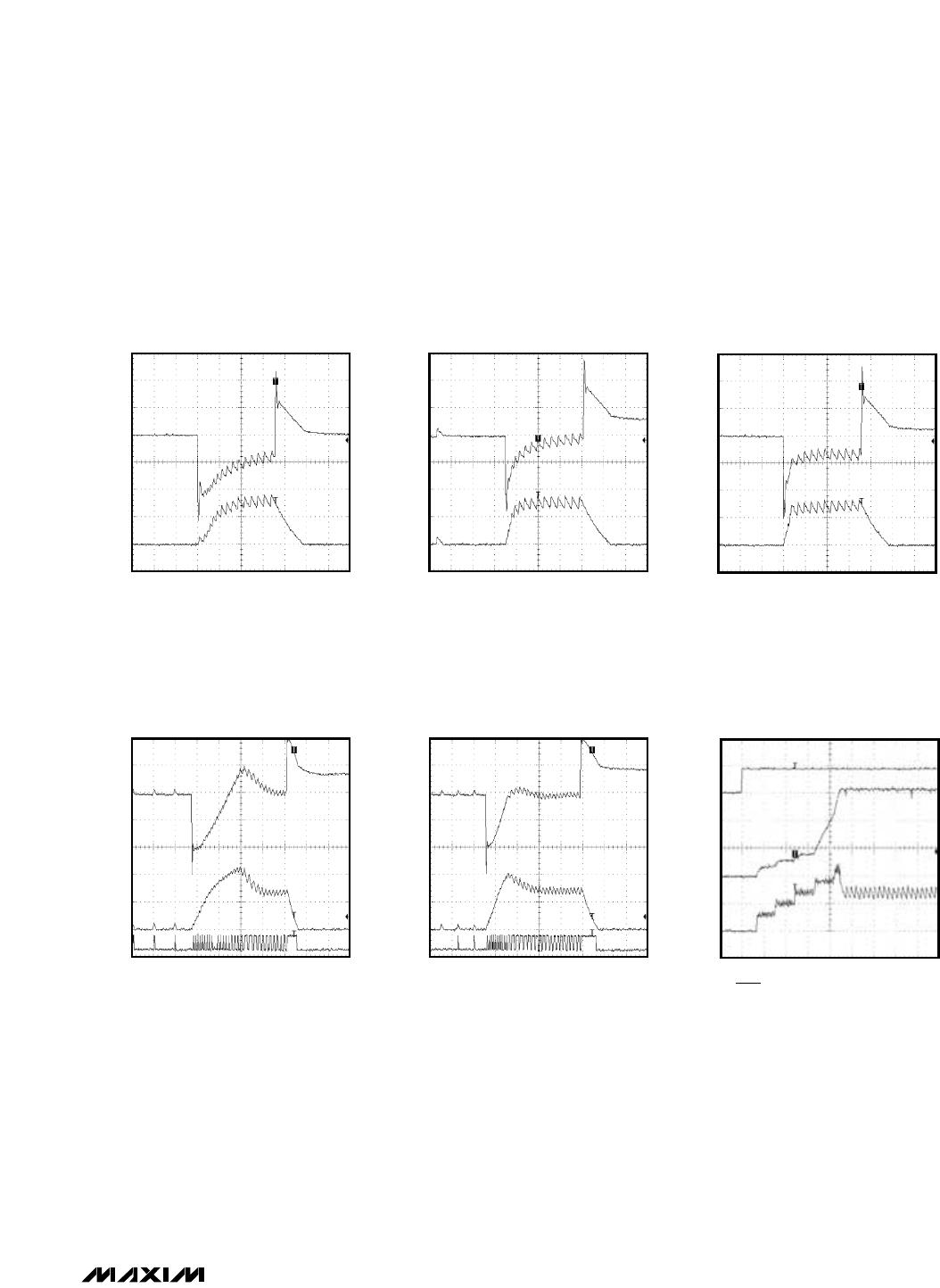
10µs/div
LOAD-TRANSIENT RESPONSE
(WITH INTEGRATOR)
V
IN
= 15V, V
O
= 1.6V, I
O
= 30mA TO 7A
A = V
OUT
, AC-COUPLED, 50mV/div
B = INDUCTOR CURRENT, 5A/div
A
B
MAX1710-17
MAX1710/MAX1711/MAX1712
High-Speed, Digitally Adjusted
Step-Down Controllers for Notebook CPUs
_______________________________________________________________________________________ 7
_____________________________Typical Operating Characteristics (continued)
(7A CPU supply circuit of Figure 1, T
A
= +25°C, unless otherwise noted.)
20µs/div
LOAD-TRANSIENT RESPONSE
(WITH INTEGRATOR)
V
IN
= 4.5V, V
O
= 2V, I
O
= 30mA TO 7A
A = V
OUT
, AC-COUPLED, 50mV/div
B = INDUCTOR CURRENT, 5A/div
C = DL, 10V/div
A
B
C
MAX1710-19
20µs/div
LOAD-TRANSIENT RESPONSE
(WITH INTEGRATOR)
V
IN
= 4.5V, V
O
= 1.3V, I
O
= 30mA TO 7A
A = V
OUT
, AC-COUPLED, 50mV/div
B = INDUCTOR CURRENT, 5A/div
C = DL, 10V/div
A
B
C
MAX1710-20
500µs/div
STARTUP WAVEFORM
A = SHDN
B = V
OUT
, 0.5V/div
C = INDUCTOR CURRENT, 5A/div
A
B
C
MAX1710-21
10µs/div
LOAD-TRANSIENT RESPONSE
(WITHOUT INTEGRATOR)
V
IN
= 15V, V
O
= 1.6V, I
O
= 30mA TO 7A
A = V
OUT
, AC-COUPLED, 50mV/div
B = INDUCTOR CURRENT, 5A/div
A
B
MAX1710-18
MAX1710/MAX1711/MAX1712
High-Speed, Digitally Adjusted
Step-Down Controllers for Notebook CPUs
8 _______________________________________________________________________________________
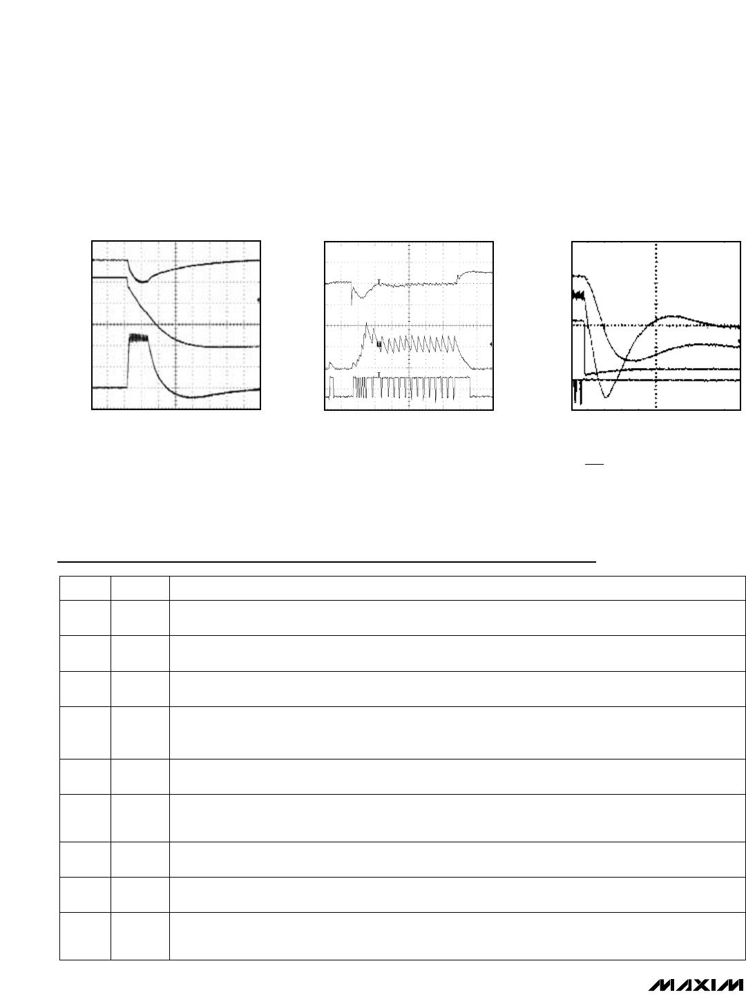
50µs/div
OUTPUT OVERLOAD WAVEFORM
V
OUT
= 1.6V
A = V
IN
, AC-COUPLED, 2V/div
B = V
OUT
, 0.5V/div
C = INDUCTOR CURRENT, 5A/div
A
B
C
MAX1710-22
5µs/div
LOAD-TRANSIENT RESPONSE
L = 0.7µH, V
OUT
= 1.6V, V
IN
= 15V, C
OUT
= 47µF (x4), f = 550kHz
A = V
OUT
, AC-COUPLED, 100mV/div
B = INDUCTOR CURRENT, 5A/div
C = DL, 5V/div
A
B
C
MAX1710-23
CERAMIC C
OUT
5µs/div
SHUTDOWN WAVEFORM
V
IN
= 15V, V
0
= 1.6V, I
0
= 7A
A = V
OUT
, 0.5V/div
B = INDUCTOR CURRENT, 5A/div
C = SHDN, 2V/div
D = DL, 5V/div
A
B
C
D
MAX1710-24
_____________________________Typical Operating Characteristics (continued)
(7A CPU supply circuit of Figure 1, T
A
= +25°C, unless otherwise noted.)
Pin Description
NAME FUNCTION
5 CC
Integrator Capacitor Connection. Connect a 100pF to 1000pF (470pF typical) capacitor to GND to set the
integration time constant.
PIN
4 FBS
Feedback Remote-Sense Input, normally connected to V
OUT
directly at the load. FBS internally connects to
the integrator that fine tunes the DC output voltage. Tie FBS to V
CC
to disable all three integrator amplifiers.
Tie FBS to FB (or disable the integrators) when externally adjusting the output voltage with a resistor-divider.
3 FB
Fast Feedback Input, normally connected to V
OUT
. FB is connected to the bulk output filter capacitors local-
ly at the power supply. An external resistor-divider can optionally set the output voltage.
8 TON
On-Time Selection Control Input. This is a four-level input that sets the K factor to determine DH on-time.
GND = 550kHz, REF = 400kHz, open = 300kHz, V
CC
= 200kHz.
7 V
CC
Analog Supply Voltage Input for PWM Core, 4.5V to 5.5V. Bypass V
CC
to GND with a 0.1µF minimum
capacitor.
6 ILIM
Current-Limit Threshold Adjustment. Connects to an external resistor to GND. The LX-PGND current-limit
threshold defaults to +100mV if ILIM is tied to V
CC
. The current-limit threshold is 1/10 of the voltage forced at
ILIM. In adjustable mode, the threshold is V
TH
= R
LIM
5µA/10.
1 V+
Battery Voltage Sense Connection. V+ is used only for PWM one-shot timing. DH on-time is inversely propor-
tional to V+ input voltage over a range of 2V to 28V.
9 REF
2.0V Reference Output. Bypass REF to GND with a 0.22µF minimum capacitor. REF can source 50µA for
external loads. Loading REF degrades FB accuracy according to the REF load-regulation error
(see Electrical Characteristics).
2
SHDN
Shutdown Control Input, active low. SHDN cannot withstand the battery voltage. In shutdown mode, DL is
forced to V
DD
in order to enforce overvoltage protection, even when powered down (unless OVP is high).
MAX1710/MAX1711/MAX1712
High-Speed, Digitally Adjusted
Step-Down Controllers for Notebook CPUs
_______________________________________________________________________________________ 9
Standard Application Circuit
The standard application circuit (Figure 1) generates a
low-voltage, high-power rail for supplying up to 7A to the
core CPU V
CC
in a notebook computer. This DC-DC
converter steps down a battery or AC adapter voltage to
sub-2V levels with high efficiency and accuracy, and
represents a good compromise between size, efficiency,
and cost.
See the MAX1710 EV kit manual for a list of components
and suppliers.
Detailed Description
The MAX1710/MAX1711/MAX1712 buck controllers are
targeted for low-voltage, high-current CPU power sup-
plies for notebook computers. CPU cores typically exhib-
it 0A to 10A or greater load steps when the clock is
throttled. The proprietary Quick-PWM pulse-width modu-
lator in the MAX1710/MAX1711/MAX1712 is specifically
designed for handling these fast load steps while main-
taining a relatively constant operating frequency and
inductor operating point over a wide range of input volt-
ages. The Quick-PWM architecture circumvents the poor
load-transient timing problems of fixed-frequency cur-
Pin Description (continued)
NAME FUNCTION
16
(MAX1711/
MAX1712)
D4 DAC Code Input, MSB. 5µA internal pullup to V
CC
(Tables 1, 2, and 3).
PIN
13 DL Low-Side Gate-Driver Output, swings 0 to V
DD
12 PGOOD Open-Drain Power-Good Output
11 GNDS
Ground Remote-Sense Input, normally connected to ground directly at the load. GNDS internally con-
nects to the integrator that fine tunes the ground offset voltage.
10 GND Analog Ground
14 PGND Power Ground. Also used as the inverting input for the current-limit comparator.
15 V
DD
Supply Voltage Input for the DL Gate Driver, 4.5V to 5.5V
17 D3 DAC Code Input. 5µA internal pullup to V
CC
.
16
(MAX1710)
OVP
Overvoltage-Protection Disable Control Input (Table 4). GND = normal operation and overvoltage
protection active, V
CC
= overvoltage protection disabled.
22 BST
Boost Flying-Capacitor Connection. An optional resistor in series with BST allows the DH pullup
current to be adjusted (Figure 5). This technique of slowing the LX rise time can be used to prevent
accidental turn-on of the low-side MOSFET due to excessive gate-drain capacitance.
21
SKIP
Low-Noise-Mode Selection Control Input. Low-noise forced-PWM mode causes inductor current
recirculation at light loads and suppresses pulse-skipping operation. Normal operation prevents
current recirculation. SKIP can also be used to disable both overvoltage and undervoltage protection
circuits and clear the fault latch (Figure 6). GND = normal operation, V
CC
= low-noise mode. Do not
leave SKIP floating.
20 D0 DAC Code Input LSB. 5µA internal pullup.
19 D1 DAC Code Input. 5µA internal pullup.
18 D2 DAC Code Input. 5µA internal pullup.
24 DH High-Side Gate-Driver Output. Swings LX to BST.
23 LX
Inductor Connection. LX serves as the lower supply rail for the DH high-side gate driver. Also used
for the noninverting input to the current-limit comparator, as well as the skip-mode zero-crossing com-
parator.
MAX1712EEG

Mfr. #:
Manufacturer:
Maxim Integrated
Description:
LDO Voltage Controllers High-Speed, Digitally Adjusted Step-Down Controllers for Notebook CPUs
Lifecycle:
New from this manufacturer.
Delivery:
DHL FedEx Ups TNT EMS
Payment:
T/T Paypal Visa MoneyGram Western Union

Products related to this Datasheet