MAX1710/MAX1711/MAX1712
rent-mode PWMs while also avoiding the problems
caused by widely varying switching frequencies in con-
ventional constant-on-time and constant-off-time PWM
schemes.
+5V Bias Supply (V
CC
and V
DD
)
The MAX1710/MAX1711/MAX1712 require an external
+5V bias supply in addition to the battery. Typically, this
+5V bias supply is the notebook’s 95% efficient 5V sys-
tem supply. Keeping the bias supply external to the IC
improves efficiency and eliminates the cost associated
with the +5V linear regulator that would otherwise be
needed to supply the PWM circuit and gate drivers. If
stand-alone capability is needed, the +5V supply can be
generated with an external linear regulator such as the
MAX1615.
The battery and +5V bias inputs can be tied together if
the input source is a fixed 4.5V to 5.5V supply. If the +5V
bias supply is powered up prior to the battery supply, the
enable signal (SHDN) must be delayed until the battery
voltage is present in order to ensure startup. The +5V
bias supply must provide V
CC
and gate-drive power, so
the maximum current drawn is:
High-Speed, Digitally Adjusted
Step-Down Controllers for Notebook CPUs
10 ______________________________________________________________________________________
V
CC
V
BATT
4.5V TO 28V
+5V
BIAS SUPPLY
C2
3 x 470µF
KEMET T510
PANASONIC
ETQP6F2R0HFA
POWER-GOOD
INDICATOR
*MAX1710 ONLY
**MAX1711/MAX1712 ONLY
L1
2µH
V
OUT
1.25V TO 2V AT 7A (MAX1710)
0.925V TO 2V AT 7A (MAX1711)
1.1V TO 1.85V AT 7A (MAX1712)
SHDN
V+
221
2
21
20
19
18
17
24
23
13
14
3
4
11
R4
1k
12
7
15
D2
CMPSH-3
C6
1µF
C7
0.1µF
C4
1µF
C3
470pF
TO V
CC
Q1
D1
R2
100k
D3
(OPTIONAL OVP
REVERSE-POLARITY
CLAMP)
Q2
C5
1µF
R1
20
C1 3 x 10µF/30V
SKIP
D0
D1
D2
DAC
INPUTS
ON/OFF
CONTROL
LOW-NOISE
CONTROL
DL
LX
BST
DH
PGND
FB
FBS
GNDS
Q1 = IRF7807
Q2 = IRF7805
D1, D3 = MBRS130T3 (OPTIONAL)
C1 = SANYO OS-CON (30SC10M)
PGOOD
V
DD
MAX1710
MAX1711
MAX1712
8
9
5
6
16
+5V
10
D3
16
D4**
TON
REF
CC
GND
R3
(OPTIONAL)
ILIM OVP*
Figure 1. Standard Application Circuit
I
BIAS
= I
CC
+ f
(Q
G1
+ Q
G2
) = 15mA to 30mA (typ)
where I
CC
is 600µA (typ), f is the switching frequency,
and Q
G1
and Q
G2
are the MOSFET data sheet total
gate-charge specification limits at V
GS
= 5V.
Free-Running, Constant-On-Time PWM
Controller with Input Feed-Forward
The Quick-PWM control architecture is an almost fixed-
frequency, constant-on-time current-mode type with volt-
age feed-forward (Figure 2). This architecture relies on
the filter capacitor’s ESR to act as the current-sense
resistor, so the output ripple voltage provides the PWM
ramp signal. The control algorithm is simple: the high-
side switch on-time is determined solely by a one-shot
whose period is inversely proportional to input voltage
and directly proportional to output voltage. Another one-
shot sets a minimum off-time (400ns typ). The on-time
one-shot is triggered if the error comparator is low, the
MAX1710/MAX1711/MAX1712
High-Speed, Digitally Adjusted
Step-Down Controllers for Notebook CPUs
______________________________________________________________________________________ 11
REF
-5%
FROM
D/A
REF
REF
D0 D1 D2 D3
10k
ERROR
AMP
TOFF
TON
REF
+12%
FB
REF
-30%
R-2R
D/A CONVERTER
CHIP SUPPLY
g
m
g
m
g
m
GNDS
CC
SHDN
FBS
PGOOD
OVP/UVLO
LATCH
ON-TIME
COMPUTE
TON
1-SHOT
1-SHOT
TRIG
V
BATT
2V TO 28V
TRIG
Q
Q
S
R
2V
REF
GND
REF
FB
PGND
+5V
OUTPUT
DL
V
CC
V
CC
V
DD
LX
ZERO CROSSING
CURRENT
LIMIT
DH
BST
I
LIM
R
LIM
+5V
5µA
+5V
Q
S1
Q
S2 TIMER
SKIP
OVP
TON
V+
70k
Σ
MAX1710
S
R
Q
Figure 2. MAX1710 Functional Diagram
MAX1710/MAX1711/MAX1712
High-Speed, Digitally Adjusted
Step-Down Controllers for Notebook CPUs
12 ______________________________________________________________________________________
low-side switch current is below the current-limit thresh-
old, and the minimum off-time one-shot has timed out.
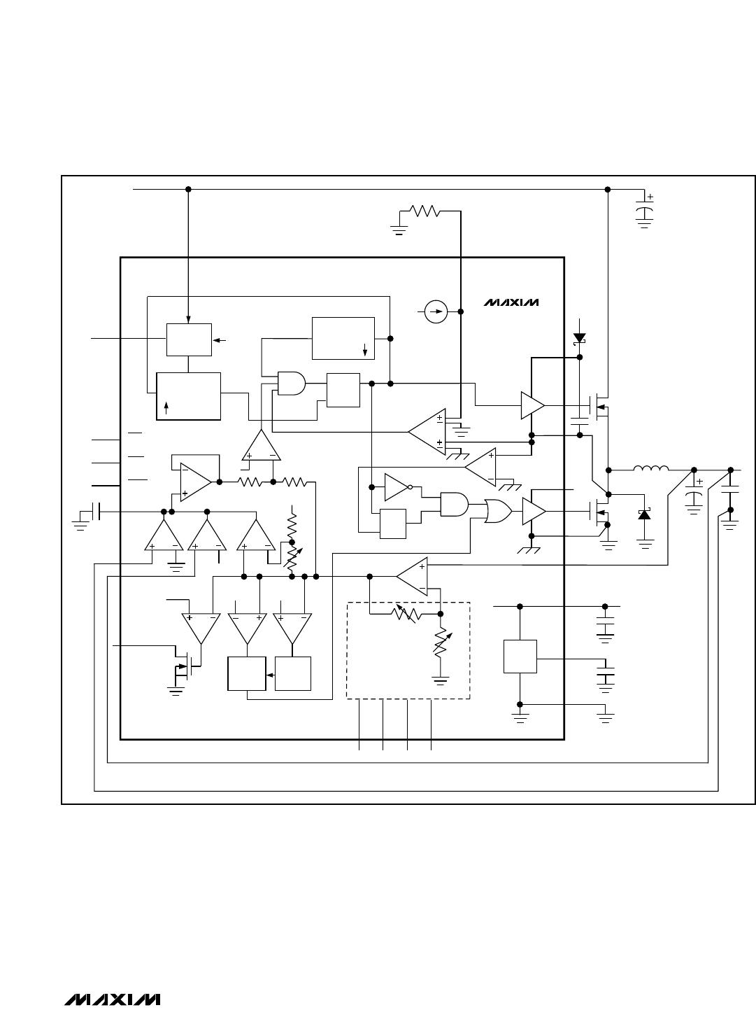
On-Time One-Shot (TON)
The heart of the PWM core is the one-shot that sets the
high-side switch on-time. This fast, low-jitter, adjustable
one-shot includes circuitry that varies the on-time in
response to battery and output voltage. The high-side
switch on-time is inversely proportional to the battery
voltage as measured by the V+ input, and directly pro-
portional to the output voltage as set by the DAC code.
This algorithm results in a nearly constant switching fre-
quency despite the lack of a fixed-frequency clock gen-
erator. The benefits of a constant switching frequency
are twofold: first, the frequency can be selected to avoid
noise-sensitive regions such as the 455kHz IF band;
second, the inductor ripple-current operating point
remains relatively constant, resulting in easy design
methodology and predictable output voltage ripple:
On-Time = K (V
OUT
+ 0.075V) / V
IN
where K is set by the TON pin-strap connection and
0.075V is an approximation to accommodate for the
expected drop across the low-side MOSFET switch.
One-shot timing error increases for the shorter on-time
settings due to fixed propagation delays and is approxi-
mately ±12.5% at 550kHz and 400kHz, and ±10% at the
two slower settings. This translates to reduced switch-
ing-frequency accuracy at higher frequencies (Table 5).
Switching frequency increases as a function of load cur-
rent due to the increasing drop across the low-side
Table 1. MAX1710 FB Output Voltage
DAC Codes
D3 D2 D1 D0
OUTPUT
VOLTAGE (V)
1 0 0 0 1.60
0 0 0 0 2.00
0 0 0 1 1.95
0 0 1 0 1.90
0 0 1 1 1.85
0 1 0 0 1.80
0 1 0 1 1.75
0 1 1 0 1.70
0 1 1 1 1.65
1 0 0 1 1.55
1 0 1 0 1.50
1 0 1 1 1.45
1 1 0 0 1.40
1 1 0 1 1.35
1 1 1 0 1.30
1 1 1 1 1.25
Table 2. MAX1711 FB Output Voltage
DAC Codes
D4 D3 D2 D1
OUTPUT
VOLTAGE (V)
0 1 0 0 1.60
0 0 0 0 2.00
0 0 0 0 1.95
0 0 0 1 1.90
0 0 0 1 1.85
0 0 1 0 1.80
0 0 1 0 1.75
0 0 1 1 1.70
0 0 1 1 1.65
0 1 0 0 1.55
0 1 0 1 1.50
0 1 0 1 1.45
0 1 1 0 1.40
0 1 1 0 1.35
0 1 1 1 1.30
0 1 1 1 Shutdown3*
1 1 0 0 1.075
1 0 0 0 1.275
1 0 0 0 1.250
1 0 0 1 1.225
1 0 0 1 1.200
1 0 1 0 1.175
1 0 1 0 1.150
1 0 1 1 1.125
1 0 1 1 1.100
1 1 0 0 1.050
1 1 0 1 1.025
1 1 0 1 1.000
1 1 1 0 0.975
1 1 1 0 0.950
1 1 1 1 0.925
1 1 1 1 Shutdown3*
D0
0
0
1
0
1
0
1
0
1
1
0
1
0
1
0
1
0
0
1
0
1
0
1
0
1
1
0
1
0
1
0
1
*See Table 4.

MAX1712EEG

Mfr. #:
Manufacturer:
Maxim Integrated
Description:
LDO Voltage Controllers High-Speed, Digitally Adjusted Step-Down Controllers for Notebook CPUs
Lifecycle:
New from this manufacturer.
Delivery:
DHL FedEx Ups TNT EMS
Payment:
T/T Paypal Visa MoneyGram Western Union

Products related to this Datasheet