MAX1710/MAX1711/MAX1712
High-Speed, Digitally Adjusted
Step-Down Controllers for Notebook CPUs
______________________________________________________________________________________ 13
MOSFET, which causes a faster inductor-current dis-
charge ramp. The on-times guaranteed in the Electrical
Characteristics are influenced by switching delays in the
external high-side power MOSFET. The exact switching
frequency will depend on gate charge, internal gate
resistance, source inductance, and DH output drive
characteristics.
Two external factors that can influence switching-fre-
quency accuracy are resistive drops in the two conduc-
tion loops (including inductor and PC board resistance)
and the dead-time effect. These effects are the largest
contributors to the change of frequency with changing
load current. The dead-time effect is a notable disconti-
nuity in the switching frequency as the load current is
varied (see Typical Operating Characteristics). It occurs
whenever the inductor current reverses, most commonly
at light loads with SKIP high. With reversed inductor cur-
rent, the inductor’s EMF causes LX to go high earlier
than normal, extending the on-time by a period equal to
the low-to-high dead time. For loads above the critical
conduction point, the actual switching frequency is:
where V
DROP1
is the sum of the parasitic voltage drops
in the inductor discharge path, including synchronous
rectifier, inductor, and PC board resistances; V
DROP2
is the sum of the resistances in the charging path,
and t
ON
is the on-time calculated by the MAX1710/
MAX1711/MAX1712.
Integrator Amplifiers (CC)
There are three integrator amplifiers that provide a fine
adjustment to the output regulation point. One amplifier
monitors the difference between GNDS and GND, while
another monitors the difference between FBS and FB.
The third amplifier integrates the difference between
REF and the DAC output. These three transconductance
amplifiers’ outputs are directly summed inside the chip,
so the integration time constant can be set easily with a
capacitor. The g
m
of each amplifier is 160µmho (typ).
The integrator block has an ability to move and correct
the output voltage by about -2%, +4%. For each amplifi-
er, the differential input voltage range is about ±50mV
total, including DC offset and AC ripple. The voltage
gain of each integrator is about 80V/V.
The FBS amplifier corrects for DC voltage drops in PC
board traces and connectors in the output bus path
between the DC-DC converter and the load. The GNDS
amplifier performs a similar DC correction task for the
output ground bus. The third amplifier provides an aver-
aging function that forces V
OUT
to be regulated at the
average value of the output ripple waveform. If the inte-
grator amplifiers are disabled, V
OUT
is regulated at the
valleys of the output ripple waveform. This creates a
slight load-regulation characteristic in which the output
f
VV
tV V
OUT DROP
ON IN DROP
=
+
+
()
1
2
Table 3. MAX1712 FB Output Voltage
DAC Codes (VRM 9.0)
*See Table 4.
1
0
1
0
1
0
1
1
0
1
0
1
0
1
0
0
1
0
1
0
1
0
1
1
0
1
0
1
0
1
0
0
D0
Shutdown3* 1111
1.1001111
1.1250111
1.1500111
1.1751011
1.2001011
1.2250011
1.2751101
1.3001101
1.3250101
1.3500101
1.3751001
1.4001001
1.4250001
1.4500001
1.2500011
1.475 1110
1.5001110
1.5250110
1.5500110
1.5751010
1.6001010
1.6250010
1.6751100
1.7001100
1.7250100
1.7500100
1.7751000
1.8001000
1.8250000
1.8500000
1.6500010
OUTPUT
VOLTAGE (V)
D1D2D3D4
MAX1710/MAX1711
High-Speed, Digitally Adjusted
Step-Down Controllers for Notebook CPUs
14 ______________________________________________________________________________________
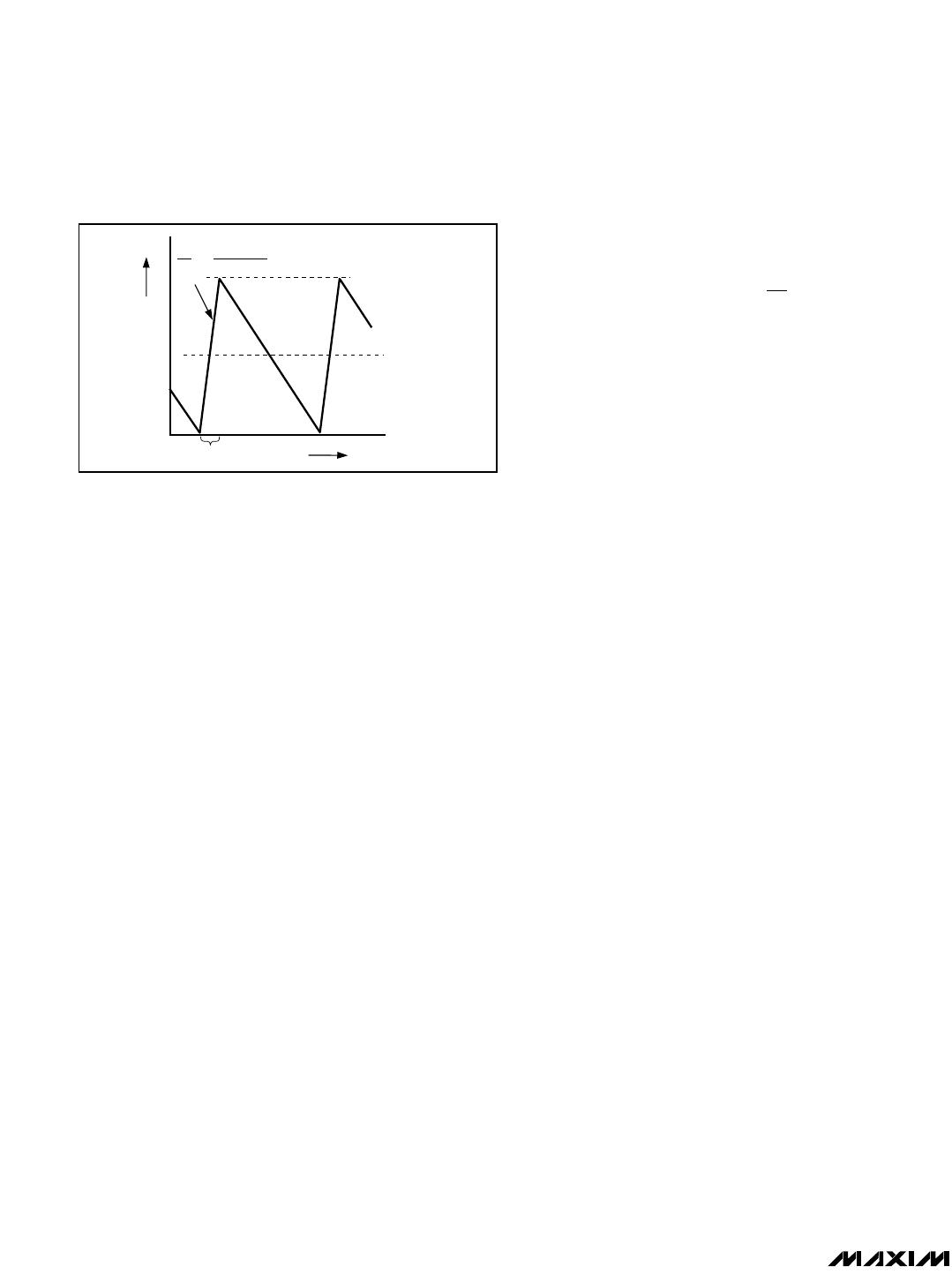
voltage rises approximately 1% (up to 1/2 the peak
amplitude of the ripple waveform as a limit) when under
light loads.
Integrators have both beneficial and detrimental char-
acteristics. While they do correct for drops due to DC
bus resistance and tighten the DC output voltage toler-
ance limits by averaging the peak-to-peak output
ripple, they can interfere with achieving the fastest pos-
sible load-transient response. The fastest transient
response is achieved when all three integrators are dis-
abled. This works very well when the MAX1710/
MAX1711/MAX1712 circuit can be placed very close to
the CPU.
There is often a connector, or at least many milliohms of
PC board trace resistance, between the DC-DC convert-
er and the CPU. In these cases, the best strategy is to
place most of the bulk bypass capacitors close to the
CPU, with just one capacitor on the other side of the con-
nector near the MAX1710/MAX1711/MAX1712 to control
ripple if the CPU card is unplugged. In this situation, the
remote-sense lines and integrators provide a real benefit.
When FBS is connected to V
CC
so that all three integra-
tors are disabled, CC can be left unconnected, which
eliminates a component.
Automatic Pulse-Skipping Switchover
At light loads, an inherent automatic switchover to PFM
takes place. This switchover is effected by a comparator
that truncates the low-side switch on-time at the inductor
current’s zero crossing. This mechanism causes the
threshold between pulse-skipping PFM and nonskipping
PWM operation to coincide with the boundary between
continuous and discontinuous inductor-current operation
(also known as the “critical conduction” point;
see Continuous to Discontinuous Inductor Current Point
vs. Input Voltage graph in the Typical Operating
Characteristics). For a battery range of 7V to 24V, this
threshold is relatively constant, with only a minor depen-
dence on battery voltage.
where K is the On-Time Scale factor (Table 6). The load-
current level at which PFM/PWM crossover occurs,
I
LOAD(SKIP)
, is equal to 1/2 the peak-to-peak ripple cur-
rent, which is a function of the inductor value (Figure 3).
For example, in the standard application circuit with t
ON
= 300ns at 24V, V
OUT
= 2V, and L = 2µH, switchover to
pulse-skipping operation occurs at I
LOAD
= 1.65A or
about 1/4 full load. The crossover point occurs at an
even lower value if a swinging (soft-saturation) inductor
is used.
The switching waveforms may appear noisy and asyn-
chronous when light loading causes pulse-skipping
operation, but this is a normal operating condition that
results in high light-load efficiency. Trade-offs in PFM
noise vs. light-load efficiency can be made by varying
the inductor value. Generally, low inductor values pro-
duce a broader efficiency vs. load curve, while higher
values result in higher full-load efficiency (assuming that
the coil resistance remains fixed) and less output voltage
ripple. Penalties for using higher inductor values include
larger physical size and degraded load-transient
response (especially at low input voltage levels).
Forced-PWM Mode (
SSKKIIPP
= High)
The low-noise, forced-PWM mode (SKIP driven high) dis-
ables the zero-crossing comparator, which controls the
low-side switch on-time. This causes the low-side gate-
drive waveform to become the complement of the high-
side gate-drive waveform. This in turn causes the
inductor current to reverse at light loads, as the PWM
loop strives to maintain a duty ratio of V
OUT
/V
IN
. The
benefit of forced-PWM mode is to keep the switching fre-
quency fairly constant, but it comes at a cost: the no-
load battery current can be as high as 40mA or more.
Forced-PWM mode is most useful for reducing audio-fre-
quency noise, improving load-transient response, pro-
viding sink-current capability for dynamic output voltage
adjustment, and improving the cross-regulation of multi-
ple-output applications that use a flyback transformer or
coupled inductor.
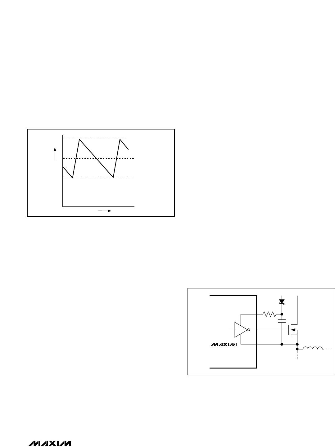
Current-Limit Circuit (ILIM)
The current-limit circuit employs a unique “valley” cur-
rent-sensing algorithm that uses the on-state resistance
of the low-side MOSFET as a current-sensing element. If
the current-sense signal is above the current-limit
threshold, the PWM is not allowed to initiate a new cycle
(Figure 4). The actual peak current is greater than the
current-limit threshold by an amount equal to the induc-
I
K
L
LOAD SKIP
()
2
Figure 3. Pulse-Skipping/Discontinuous Crossover Point
INDUCTOR CURRENT
I
LOAD
= I
PEAK
/2
ON-TIME0 TIME
-I
PEAK
L
V
BATT
- V
OUT
i
t
=
MAX1710/MAX1711/MAX1712
High-Speed, Digitally Adjusted
Step-Down Controllers for Notebook CPUs
______________________________________________________________________________________ 15
tor ripple current. Therefore the exact current-limit char-
acteristic and maximum load capability are a function of
the MOSFET on-resistance, inductor value, and battery
voltage. The reward for this uncertainty is robust, loss-
less overcurrent sensing. When combined with the UVP
protection circuit, this current-limit method is effective in
almost every circumstance.
There is also a negative current limit that prevents exces-
sive reverse inductor currents when V
OUT
is sinking cur-
rent. The negative current-limit threshold is set to
approximately 120% of the positive current limit, and
therefore tracks the positive current limit when ILIM is
adjusted.
The current-limit threshold can be adjusted with an exter-
nal resistor (R
LIM
) at ILIM. A precision 5µA pullup current
source at ILIM sets a voltage drop on this resistor,
adjusting the current-limit threshold from 50mV to
200mV. In the adjustable mode, the current-limit thresh-
old voltage is precisely 1/10th the voltage seen at ILIM.
Therefore, choose R
LIM
equal to 2k/mV of the current-
limit threshold. The threshold defaults to 100mV when
ILIM is tied to V
CC
. The logic threshold for switchover to
the 100mV default value is approximately V
CC
- 1V.
The adjustable current limit can accommodate
MOSFETs with atypical on-resistance characteristics
(see Design Procedure).
A capacitor in parallel with R
LIM
can provide a variable
soft-start function.
Carefully observe the PC board layout guidelines to
ensure that noise and DC errors don’t corrupt the cur-
rent-sense signals seen by LX and PGND. The IC must
be mounted close to the low-side MOSFET with short,
direct traces making a Kelvin-sense connection to the
source and drain terminals.
MOSFET Gate Drivers (DH, DL)
The DH and DL drivers are optimized for driving moder-
ate-size, high-side and larger, low-side power MOSFETs.
This is consistent with the low duty factor seen in the
notebook CPU environment, where a large V
BATT
- V
OUT
differential exists. An adaptive dead-time circuit monitors
the DL output and prevents the high-side FET from turn-
ing on until DL is fully off. There must be a low-resis-
tance, low-inductance path from the DL driver to the
MOSFET gate in order for the adaptive dead-time circuit
to work properly. Otherwise, the sense circuitry in the
MAX1710/MAX1711/MAX1712 will interpret the MOSFET
gate as “off” while there is actually still charge left on the
gate. Use very short, wide traces measuring 10 to 20
squares (50 to 100 mils wide if the MOSFET is 1 inch
from the MAX1710/MAX1711/MAX1712).
The dead time at the other edge (DH turning off) is deter-
mined by a fixed 35ns (typ) internal delay.
The internal pulldown transistor that drives DL low is
robust, with a 0.5 (typ) on-resistance. This helps pre-
vent DL from being pulled up during the fast rise time of
the inductor node, due to capacitive coupling from the
drain to the gate of the massive low-side synchronous-
rectifier MOSFET. However, you might still encounter
some combinations of high- and low-side FETs that will
cause excessive gate-drain coupling, which can lead to
efficiency-killing, EMI-producing shoot-through currents.
This can often be remedied by adding a resistor in series
with BST, which increases the turn-on time of the high-
side FET without degrading the turn-off time (Figure 5).
DAC Converter (D0–D4)
The DAC programs the output voltage. It receives a digi-
tal code from pins on the CPU module that are either
hard-wired to GND or left open-circuit. The
MAX1710/MAX1711/MAX1712 contain weak internal
BST
+5V
V
BATT
5
DH
LX
MAX1710
MAX1711
MAX1712
Figure 5. Reducing the Switching-Node Rise Time
Figure 4.”Valley’’ Current-Limit Threshold Point
INDUCTOR CURRENT
I
LIMIT
I
LOAD
0 TIME
LX-PGND I
LIMIT
THRESHOLD = 100mV (NOMINAL, DEFAULT)
VOLTAGE DROP ACROSS Q2
-I
PEAK

MAX1712EEG

Mfr. #:
Manufacturer:
Maxim Integrated
Description:
LDO Voltage Controllers High-Speed, Digitally Adjusted Step-Down Controllers for Notebook CPUs
Lifecycle:
New from this manufacturer.
Delivery:
DHL FedEx Ups TNT EMS
Payment:
T/T Paypal Visa MoneyGram Western Union

Products related to this Datasheet