©2013 Silicon Storage Technology, Inc. DS-20005014B 11/2013
10
16 Mbit Multi-Purpose Flash Plus
SST39WF1601 / SST39WF1602
Data Sheet
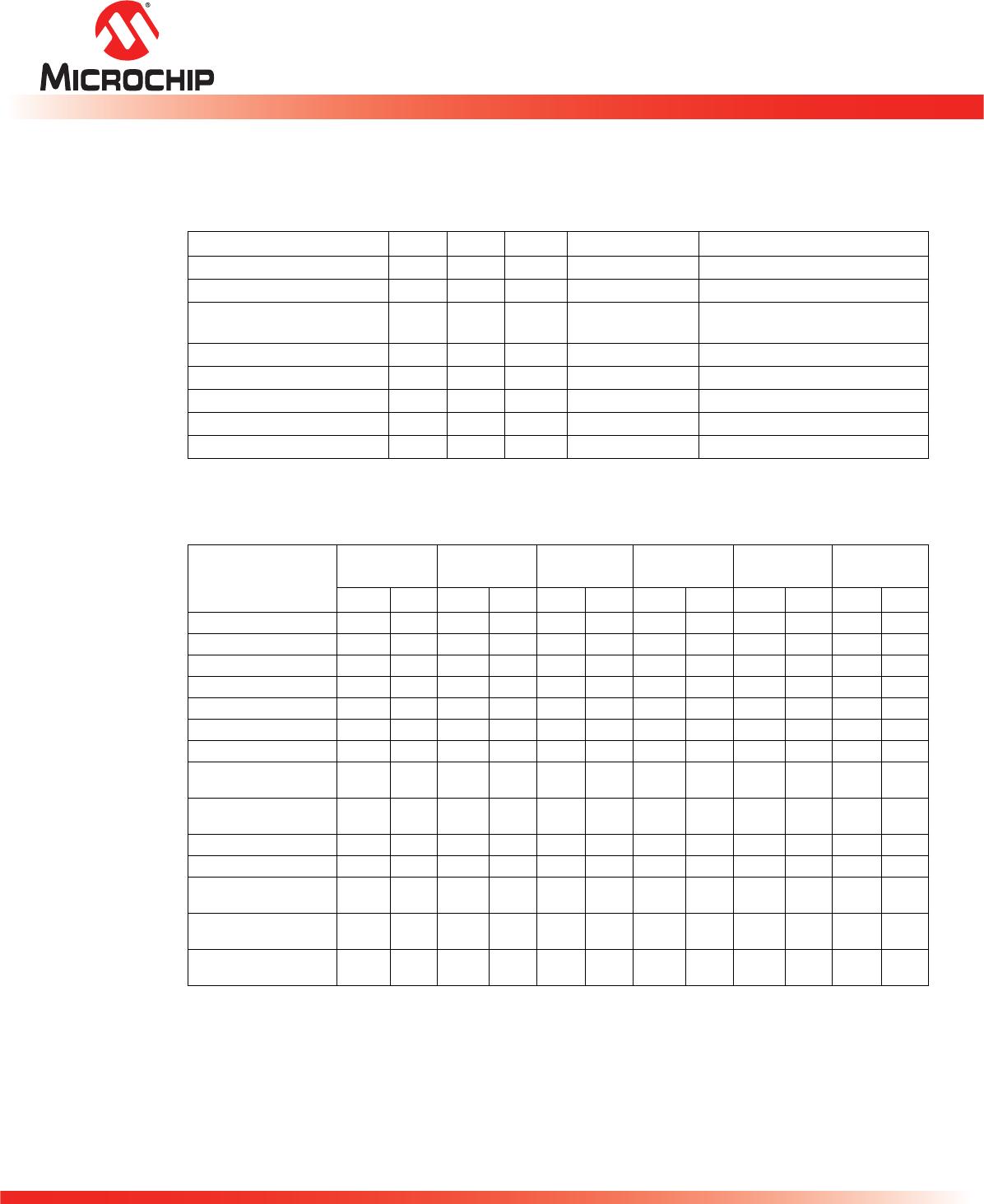
Common Flash Memory Interface (CFI)
The SST39WF1601/1602 contain the CFI information to describe the characteristics of the device. The
SST39WF1601/1602 support the original SST CFI Query mode implementation for compatibility with
existing SST devices as well as the general CFI Query mode. Both will be explained in subsequent
paragraphs.
In order to enter the SST CFI Query mode, the system must write the three-byte sequence, same as
the product ID entry command with 98H (CFI Query command) to address 5555H in the last byte
sequence. Once the device enters CFI Query mode, the system can read CFI data at the addresses
given in Tables 7 through 9. The system must write the CFI Exit command to return to Read mode from
the CFI Query mode.
In order to enter the general CFI Query mode, the system must write a one-byte sequence with entry
command with 98H to address 55H. Once the device enters the CFI Query mode, the system can read
CFI data at the addresses given in Tables 7 through 9. The system must write the CFI Exit command to
return to Read mode from the CFI Query mode.
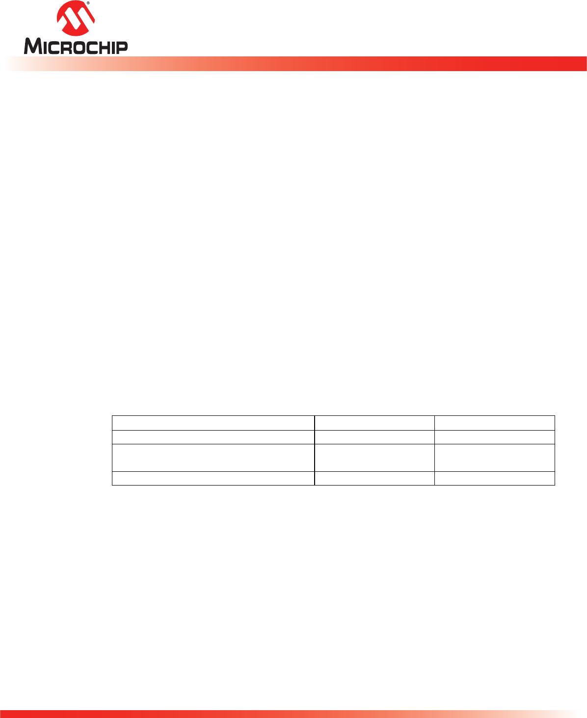
Product Identification
The Product Identification mode identifies the devices as the SST39WF1601, SST39WF1602 and
manufacturer as SST. This mode may be accessed software operations. Users may use the Software
Product Identification operation to identify the part (i.e., using the device ID) when using multiple man-
ufacturers in the same socket. For details, see Table 6 for software operation, Figure 12 for the Soft-
ware ID Entry and Read timing diagram and Figure 22 for the Software ID Entry command sequence
flowchart.
Product Identification Mode Exit/CFI Mode Exit
In order to return to the standard Read mode, the Software Product Identification mode must be exited.
Exit is accomplished by issuing the Software ID Exit command sequence, which returns the device to
the Read mode. This command may also be used to reset the device to the Read mode after any inad-
vertent transient condition that apparently causes the device to behave abnormally, e.g., not read cor-
rectly. Please note that the Software ID Exit/CFI Exit command is ignored during an internal Program
or Erase operation. See Table 6 for software command codes, Figure 14 for timing waveform, and Fig-
ures 22 and 23 for flowcharts.
Table 4: Product Identification
Address Data
Manufacturer’s ID 0000H BFH
Device ID
SST39WF1601 0001H BF274B
SST39WF1602 0001H BF274A
T4.0 20005014