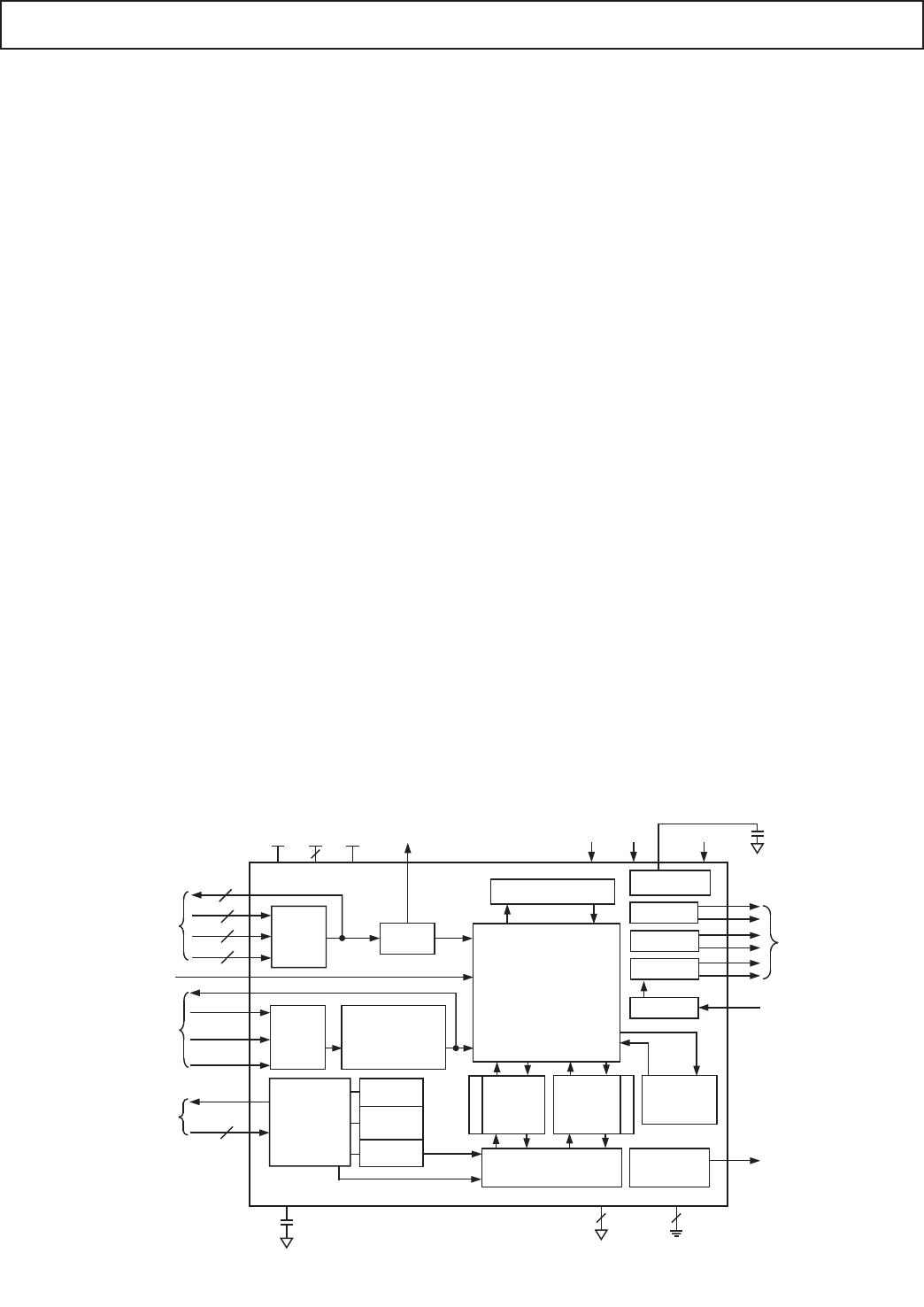
AD1953
–9–
PRODUCT OVERVIEW (continued from page 1)
An extensive SPI port allows click-free parameter updates, along
with readback capability from any point in the algorithm flow.
The AD1953 also includes ADI’s patented multibit Σ-Δ DAC
architecture. This architecture provides 112 dB SNR and dynamic
range and THD+N of –100 dB. These specifications allow the
AD1953 to be used in applications ranging from low end
boom-boxes to high end professional mixing/editing systems.
The AD1953 has a digital output that allows it to be used purely
as a DSP. This digital output can also be used to drive an exter-
nal DAC to extend the number of channels beyond the three
that are provided on the chip. This chip can be used with either
its default signal processing program or with a custom user-
designed program. Graphical programming tools are available
from ADI for custom programming.
Features
The AD1953 is comprised of a 26-bit DSP (48-bit with double-
precision) for interpolation and audio processing, three multibit
Σ-Δ modulators, and analog output drive circuitry. Other features
include an on-chip parameter RAM using a “safe-upload” feature
for transparent and simultaneous updates of filter coefficients.
Digital de-emphasis filters are also included. On-chip input
selectors allow up to three sources of serial data and master
clock to be selected. The 3-channel configuration is especially
useful for 2.1 playback systems that include two
satellite speakers
and a subwoofer. The default program
allows for independent
equalization and compression/limiting for the satellite and
subwoofer outputs. Figure 1 shows the block diagram of the device.
The AD1953 contains a program RAM that is booted from an
internal program ROM on power-up. Signal-processing param-
eters are stored in a 256-location parameter RAM, which is
initialized on power-up by an internal boot ROM. New values
are written to the parameter RAM using the SPI port. The
values stored in the parameter RAM control the IIR equalization
filters, the dual-band compressor/limiter, the delay values, and
the settings of the stereo spreading algorithm.
The AD1953 has a very sophisticated SPI port that supports
complete read/write capability of both the program RAM and
the parameter RAM. Two control registers are also provided to
control the chip serial modes and various other optional fea-
tures. Handshaking is included for ease of memory uploads/
downloads.
The AD1953 contains eight independent data-capture circuits
that can be programmed to tap the signal flow of the processor
at any point in the DSP algorithm flow. Two of these data-
capture circuits can be read back over the SPI port, and the
other six are fed to a serial output pin operating either in TDM
mode (for all six channels) or 2-channel mode for simple con-
nection to an external DAC. This allows the basic functionality
of the AD1953 to be easily extended.
The processor core in the AD1953 has been designed from the
ground up for straightforward coding of sophisticated compres-
sion/limiting algorithms. The AD1953 contains two independent
compressor/limiters with rms based amplitude detection and
attack/hold/release controls, together with an arbitrary compres-
sion curve that is loaded by the user into a lookup table that
resides in the parameter RAM. The compressor also features
look-ahead compression, which prevents compressor overshoots.
The AD1953 has a very flexible serial data input port that allows
for glueless interconnection to a variety of ADCs, DSP chips,
AES/EBU receivers, and sample rate converters. The AD1953
can be configured in left-justified, I
2
S, right-justified, or DSP
serial port compatible modes. It can support 16, 20, and 24 bits
in all modes. The AD1953 accepts serial audio data in MSB
first, twos complement format. The part can also be set up in a
4-channel serial input mode by simultaneously using the serial
input mux and the auxiliary serial input.
The AD1953 operates from a single 5 V power supply. It is
fabricated on a single monolithic integrated circuit and is housed
in a 48-lead LQFP package for operation over the temperature
range –40°C to +105°C.
3:1
AUDIO
DATA
MUX
1
3
3
SPI PORT
3:1
MCLK
MUX
1
MCLK
GENERATOR
1
(256/512 f
S
IN)
256/512 f
S
OUT
DAC L
COEFFICIENT
ROM
64 22
26 22
DSP CORE
DATA FORMAT:
3.23 (SINGLE PRECISION)
3.45 (DOUBLE PRECISION)
3
3
ANALOG
OUTPUTS
MASTER
CLOCK I/O
GROUP
DCSOUT
SPI I/O
GROUP
3
SERIAL
IN
1
DATA MEMORY, 512 26
CONTROL
REGISTERS
TRAP REG.
(I
2
S, SPI)
SAFELOAD
REGISTERS
PROGRAM
RAM
512 35
PARAMETER
RAM
256 22
BOOT ROM
MEMORY CONTROLLERS
DAC R
DACSW
2
BIAS
ANALOG
BIAS
RESETB MUTE DE-EMPHASISZEROFLAG
NOTES
1
CONTROLLED THROUGH SPI CONTROL REGISTERS
2
DAC DOES NOT USE DIGITAL INTERPOLATION
SERIAL DATA I/O
GROUP
DCSOUT TRAP
AUX SERIAL
DATA INPUT
(2-CHANNEL
AND TDM)
FILTCAP AGND
3
DGND
2
VO LTAG E
REFERENCE
VREF
DVDD AVDD ODVDD
3
BOOT ROM
Figure 1. Block Diagram
REV. A
AD1953
–10–
Pin Functions
All input pins have a logic threshold compatible with TTL input
levels, and may therefore be used in systems with 3.3 V logic.
All digital output levels are controlled by the ODVDD pin,
which may range from 2.7 V to 5.5 V, for compatibility with a
wide range of external devices. (See Pin Function Descriptions.)
SDATA0, 1, 2—Serial Data Inputs.
One of these three inputs is selected by an internal MUX, set by
writing to Bits <7:6> in Control Register 2. Default is 00, which
selects SDATA0. The serial format is selected by writing to Bits
<3:0> of Control Register 0. See SPI Read/Write Data Formats
section for recommendations on how to change input sources
without causing a click or pop noise.
LRCLK0, 1, 2—Left/Right Clocks for Framing the Input Data.
The active LRCLK input is selected by writing to Bits <7:6>
in Control Register 2. Default is 00, which selects LRCLK0.
The interpretation of the LRCLK changes according to the serial
mode, set by writing to Control Register 0.
BCLK0, 1, 2—Serial Bit Clocks for Clocking in the Serial Data.
The active BCLK input is selected by writing to Bits <7:6> in
Control Register 2. Default is 00, which selects BCLK0. The
interpretation of BCLK changes according to the serial mode,
which is set by writing to Control Register 0.
DMUXO/TDMO, LRMUXO/TDMFS, BMUXO/TDMBC
Dual-function pins:
Function 1: Outputs of 3:1 MUX that selects one of the
three serial input groups.
Function 2: Used for 6-channel data capture outputs in
TDM Data Capture Mode.
These three pins operate as MUX outputs when Bit <8> of
Control Register 2 is a 1 and Bits <13:12> of Control Register 1
are 00. These pins may be used to send the selected serial input
signals to other external devices. The default is OFF.
In TDM mode, TDMBC provides a 256
×
f
S
clock signal,
TDMFS provides a frame sync signal, and TDMO provides the
TDM data for an external multichannel DAC or CODEC, such
as the AD1833 or AD1836 respectively. These output pins are
enabled by writing a 01 to Bits <13:12> of Control Register 1.
The default mode is 00, or OFF.
In TDM mode, the internal signals that are captured are con-
trolled by writing Program Counter Trap numbers to SPI
addresses 268 to 273. When the internal Program Counter
contents are equal to the Trap values written to the SPI port, the
selected DSP register is transferred to parallel-to-serial registers
and shifted out of the TDMO pin.
MCLK0, 1, 2—Master Clock Inputs.
Active input selected by writing to Bits <5:4> of Control Regis-
ter 2. The default is 00, which selects MCLK0. The master clock
frequency must be either 256 × f
S
or 512 × f
S
, where f
S
is the input
sampling rate. The master clock frequency is programmed by
writing to Bit <2> of Control Register 2. The default is 0, (512
× f
S
). See Initialization section for recommendations concerning
how to change clock sources without causing an audio click or
pop. Note that since the default MCLK source pin is MCLK0,
there must be a clock signal present on this pin on power-up so
that the AD1953 can complete its initialization routine.
MCLKO—Master Clock Output.
The master clock output pin may be programmed to produce
either 256 × f
S
, 512 × f
S
, or a copy of the selected MCLK input
pin. This pin is programmed by writing to Bits <1:0> of Control
Register 2. The default is 00, which disables the MCLKO pin.
CDATA—Serial Data In for the SPI Control Port.
See SPI Port section for more information on SPI port timing.
COUT—Serial Data Output.
This is used for reading back registers and memory locations. It
is three-stated when an SPI read is not active. See SPI Port
section for more information on SPI port timing.
CCLK—SPI Bit Rate Clock.
This pin either may run continuously or be gated off between
SPI transactions. See SPI Port section for more information on
SPI port timing.
CLATCH—SPI Latch Signal.
This pin must go LOW at the beginning of an SPI transaction,
and HIGH at the end of a transaction. Each SPI transaction
may take a different number of CCLKs to complete, depending
on the address and read/write bit that are sent at the beginning
of the SPI transaction. Detailed SPI timing information is given
in the SPI Port section.
RESETB—Active-Low Reset Signal.
After RESETB goes HIGH, the AD1953 goes through an ini-
tialization sequence where the program and parameter RAMs
are initialized with the contents of the on-board boot ROMs. All
SPI registers are set to 0, and the data RAMs are also zeroed.
The initialization is complete after 1024 MCLK cycles. Since
the MCLK IN FREQ SELECT (Bit <2> in Control Register 2)
defaults to 512 × f
S
at power-up, this initialization will proceed
at the external MCLK rate and will take 1024 MCLK cycles to
complete, regardless of the absolute frequency of the external
MCLK. New values should not be written to the SPI port until
the initialization is complete.
ZEROFLAG—Zero-Input Indicator.
This pin will go HIGH if both serial inputs have been inactive
(zero data) for 1024 LRCLK cycles. This pin may be used to
drive an external mute FET for reduced noise during digital
silence. This pin also functions as a test out pin, controlled by
the test register at SPI address 511. While most test modes are
not useful to the end user, one may be of some use. If the test
register is programmed with the number 7 (decimal), the
ZEROFLAG output will be switched to the output of the inter-
nal pseudo-random noise generator. This noise generator
operates at a bit rate of 128 × f
S
, and has a repeat time of once
per 2
24
cycles. This mode may be used to generate white noise
(or, with appropriate filtering, pink noise) to be used as a test
signal for measuring speakers or room acoustics.
DCSOUT—Data Capture Serial Out.
This pin will output the DSP’s internal signals, which can be
used by external DACs or other signal-processing devices. The
signals that are captured and output on the DCSOUT pin are
controlled by writing Program Counter Trap numbers to SPI
addresses 263 (for the left output) and 264 (for the right output).
When the internal Program Counter contents are equal to the
Trap values written to the SPI port, the selected DSP register is
transferred to the DCSOUT parallel-to-serial registers and
REV. A
AD1953
–11–
shifted out on the DCSOUT pin. Table XXI shows the Pro-
gram Counter Trap values and register-select values that should
be used to tap various internal points of the algorithm flow.
The DCSOUT pin is meant to be used in conjunction with the
LRCLK and BCLK signals that are provided to the serial input
port. The format of DCSOUT is the same as the format used
for the serial port. In other words, if the serial port is running in
I
2
S mode, then the DCSOUT pin, together with the LRCLK0
and BCLK0 pins (assuming input 0 is selected), will form a
valid 3-wire I
2
S output.
The DCSOUT pin can be used for a variety of purposes. If the
DCSOUT pin is used to drive another external DAC, then a 4.1
system is possible using a new program downloaded into the
program RAM.
AUXDATA—Auxiliary Serial Data Input.
The AUXDATA pin may be used in conjunction with a custom
program to access two extra channels of serial input data, allow-
ing for a total of four input channels. The serial format is identical
to the selected format of SDATA0, 1, 2. The AUXDATA pin is
synchronous to the selected LRCLK and BCLK signal, and there-
fore should have the same timing as the main serial input signal.
MUTE—Mute Output Signal.
When this pin is asserted HIGH, a ramp sequence is started that
gradually reduces the volume to zero. When deasserted, the
volume ramps from zero back to the original volume setting.
The ramp speed is timed so that it takes 10 ms to reach zero
volume when starting from the default 0 dB volume setting.
VOUTL+, VOUTL– —Left-Channel Differential Analog Out-
puts. Full-scale outputs correspond to 1 V rms on each output pin,
or 2 V rms differential, assuming a VREF input voltage of 2.5 V. The
full-scale swing scales directly with VREF. These outputs are
capable of driving a load of > 5 kΩ, with a maximum peak current
of 1 mA from each pin. An external third-order filter is recom-
mended for filtering out-of-band noise.
VOUTR+, VOUTR– —Right Channel Differential Outputs.
Output characteristics are the same as for VOUTL+ and VOUTL–.
VOUTS+, VOUTS– —Sub Channel Differential Outputs.
These outputs are designed to drive loads of 10 kΩ or greater,
with a peak current capability of 250 μA. This output does not
use digital interpolation, as it is intended for low frequency
application. An external third-order filter with a cutoff frequency
< 2 kHz is recommended.
VREF—Analog Reference Voltage Input.
The nominal VREF input voltage is 2.5 V; the analog gain
scales directly with the voltage on this pin. When using the
AD1953 to drive a power amplifier, it is recommended that the
VREF voltage be derived by dividing down and heavily filtering
the supply to the power amplifier. This provides a benefit if the
compressor/limiter in the AD1953 is used to prevent amplifier
clipping. In this case, if the DAC output voltage is scaled to the
amplifier power supply, a fixed compressor threshold can be
used to protect an amplifier whose supply may vary over a wide
range. Any ac signal on this pin will cause distortion, and a large
decoupling capacitor may therefore be necessary to ensure that
the voltage on VREF is clean. The input impedance of VREF is
greater than 1 MΩ.
FILTCAP—Filter Capacitor Point.
This pin is used to reduce the noise on an internal biasing point
in order to provide the highest performance. It may not be nec-
essary to connect this pin, depending on the quality of the layout
and grounding used in the application circuit.
DVDD—Digital VDD for Core.
5 V nominal.
ODVDD—Digital VDD for All Digital Outputs.
Variable from 2.7 V to 5.5 V.
DGND (2)—Digital Ground.
AVDD (3)—Analog VDD.
5 V nominal. For best results, use a separate regulator for AVDD.
Bypass capacitors should be placed close to the pins and con-
nected directly to the analog ground plane.
AGND (3)—Analog Ground.
For best performance, separate nonoverlapping analog and
digital ground planes should be used.
REV. A

AD1953YSTZRL

Mfr. #:
Manufacturer:
Analog Devices Inc.
Description:
Audio DSPs IC Digital Audio Processor
Lifecycle:
New from this manufacturer.
Delivery:
DHL FedEx Ups TNT EMS
Payment:
T/T Paypal Visa MoneyGram Western Union

Products related to this Datasheet