AD1953
–6–
ABSOLUTE MAXIMUM RATINGS
*
DVDD to DGND . . . . . . . . . . . . . . . . . . . . . . –0.3 V to +6 V
ODVDD to DGND . . . . . . . . . . . . . . . . . . . . . –0.3 V to +6 V
AVDD to AGND . . . . . . . . . . . . . . . . . . . . . . –0.3 V to +6 V
Digital Inputs . . . . . . . . . . DGND – 0.3 V to DVDD + 0.3 V
Analog Inputs . . . . . . . . . . AGND – 0.3 V to AVDD + 0.3 V
AGND to DGND . . . . . . . . . . . . . . . . . . . . –0.3 V to +0.3 V
Reference Voltage . . . . . . . . . . . . . . . . . . . (AVDD + 0.3)/2 V
Maximum Junction Temperature . . . . . . . . . . . . . . . . 125rC
Storage Temperature Range . . . . . . . . . . . . –65rC to +150rC
Soldering . . . . . . . . . . . . . . . . . . . . . . . . . . . . . . 300rC/10 sec
*Stresses above those listed under Absolute Maximum Ratings may cause perma-
nent damage to the device. This is a stress rating only; functional operation of the
device at these or any other conditions above those indicated in the operational
section of this specification is not implied. Exposure to absolute maximum rating
conditions for extended periods may affect device reliability.
Package Characteristics (48-Lead LQFP)
Min Typ Max Unit
JA
(Thermal Resistance 76 rC/W
[Junction-to-Ambient])
JC
(Thermal Resistance 17 rC/W
[Junction-to-Case])
PIN CONFIGURATION
48-Lead LQFP
36
35
34
33
32
31
30
29
28
27
26
25
13 14 15 16 17 18 19 20 21 22 23 24
1
2
3
4
5
6
7
8
9
10
11
12
48 47 46 45 44 39 38 3743 42 41 40
PIN 1
IDENTIFIER
TOP VIEW
(Not to Scale)
NC
AGND
VOUTL–
VOUTL+
AVDD
AGND
AVDD
NC
MCLK2
MCLK1
MCLK0
AUXDATA
MUTE
DVDD
NC = NO CONNECT
S DATA 2
BCLK2
LRCLK2
S DATA 1
VOUTR+
VOUTR–
AGND
VOUTS+
AD1953
BCLK1
VOUTS–
DGND
MCLKOUT
COUT
DCSOUT
ODVDD
LRMUXO/TDMFS
BMUXO/TDMBC
DMUXO/TDMO
ZEROFLAG
FILTCAP
VREF
NC
DGND
LRCLK1
S DATA 0
BCLK0
LRCLK0
C DATA
CCLK
CLATCH
RESETB
AVDD
AGND
NC
CAUTION
ESD (electrostatic discharge) sensitive device. Electrostatic charges as high as 4000 V readily
accumulate on the human body and test equipment and can discharge without detection. Although
the AD1953 features proprietary ESD protection circuitry, permanent damage may occur on
devices subjected to high energy electrostatic discharges. Therefore, proper ESD precautions are
recommended to avoid performance degradation or loss of functionality.
REV. A
AD1953
–7–
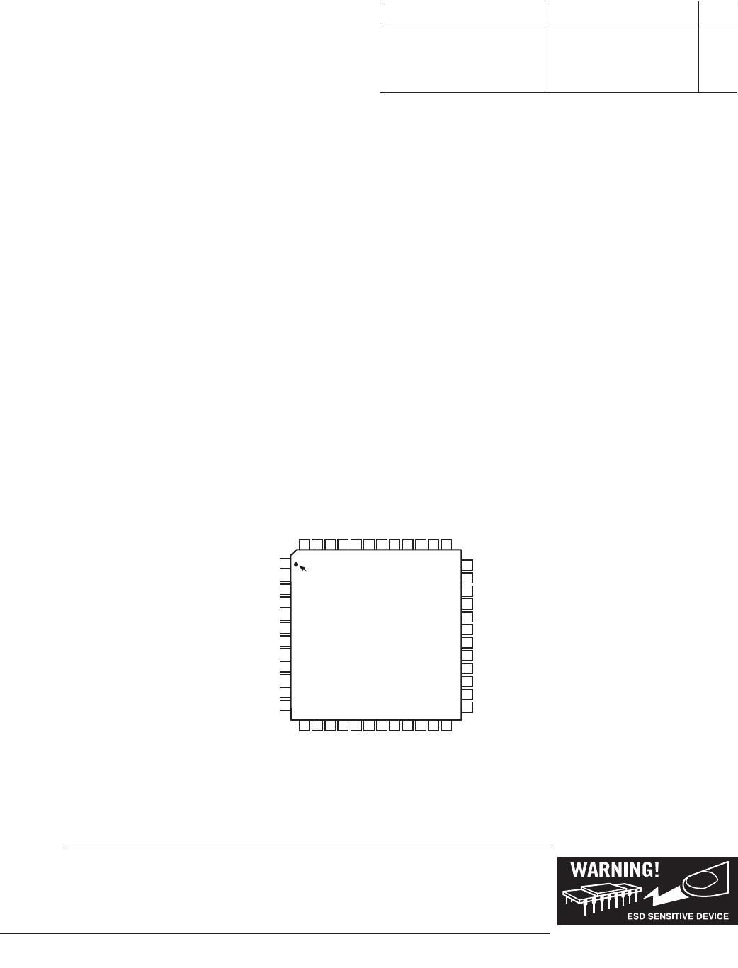
PIN FUNCTION DESCRIPTIONS
Input/
Pin No. Mnemonic Output Description
1 NC No Connect
2 MCLK2 IN Master Clock Input 2 256/512 f
S
3 MCLK1 IN Master Clock Input 1 256/512 f
S
4 MCLK0 IN Master Clock Input 0 256/512 f
S
5 AUXDATA IN Auxiliary Serial Data Input
6 MUTE IN Mute Signal, Initiates Volume Ramp-Down
7 DVDD Digital Supply for DSP Core, 4.5 V to 5.5 V
8 SDATA2 IN Serial Data Input 2
9 BCLK2 IN Bit Clock 2
10 LRCLK2 IN Left/Right Clock 2
11 SDATA1 IN Serial Data Input 1
12 BCLK1 IN Bit Clock 1
13 DGND Digital Ground
14 LRCLK1 IN Left/Right Clock 1
15 SDATA0 IN Serial Data Input 0
16 BCLK0 IN Bit Clock 0
17 LRCLK0 IN Left/Right Clock 0
18 CDATA IN SPI Data Input
19 CCLK IN SPI Data Bit Clock
20 CLATCH IN SPI Data Framing Signal
21 RESETB IN Reset Signal, Active Low
22 AVDD Analog 5 V Supply
23 AGND Analog GND
24 NC No Connect
25 VOUTS– OUT Negative Sub Analog DAC Output
26 VOUTS+ OUT Positive Sub Analog DAC Output
27 AGND Analog GND
28 VOUTR– OUT Negative Left Analog DAC Output
29 VOUTR+ OUT Positive Left Analog DAC Output
30 AVDD Analog 5 V Supply
31 AGND Analog GND
32 AVDD Analog 5 V Supply
33 VOUTL+ OUT Positive Left Analog DAC Output
34 VOUTL– OUT Negative Left Analog DAC Output
35 AGND Analog GND
36 NC No Connect
37 NC No Connect
38 VREF IN Connection for Filtered AVDD/2
39 FILTCAP IN Connection for Noise Reduction Capacitor
40 ZEROFLAG OUT Zero Flag Output. High when both left and right channels are 0 for 1024 frames.
41 DMUXO/TDMO OUT Dual-function Pin: Serial Data MUX Output/TDM Mode Output Data
42 BMUXO/TDMBC OUT Dual-function Pin: Bit Clock MUX Output/TDM Mode Bit Clock Output (256 f
S
)
43 LRMUXO/TDMFS OUT Dual-function Pin: Left/Right Clock MUX Output/TDM Mode Frame Sync
Clock Output
44 ODVDD Digital Supply Pin for Output Drivers, 2.5 V to 5.5 V
45 DCSOUT OUT Data Capture Serial Output for Data Capture Registers. Use in conjunction
with selected LRCLK and BCLK to form a 3-wire output.
46 COUT OUT SPI Data Output, Three-Stated when Inactive
47 MCLKOUT OUT Master Clock Output 512/256 f
S
(Frequency Selected by SPI Register)
48 DGND Digital Ground
REV. A
AD1953–Typical Performance Characteristics
–8–
PERFORMANCE PLOTS
The following plots demonstrate the performance achieved on the
actual silicon. TPC 1 shows an FFT of a full-scale 1 kHz signal
with a THD+N of –100 dB, which is dominated by a second
harmonic. TPC 2 shows an FFT of a –60 dB sine wave, demon-
strating the lack of low level artifacts. TPC 3 shows a frequency
response plot with the seven equalization biquads set to an alter-
nating pattern of 6 dB boosts and cuts. TPC 4 shows a linearity
plot, where the measurement was taken with the same equaliza-
tion curve used to make TPC 3. When the biquad filters are not
in use, the signal passes through the filters with no quantization
effects. TPC 4 therefore demonstrates that using double-precision
math in the biquad filters has virtually eliminated any quantization
artifacts. TPC 5 shows a tone-burst applied to the compressor,
with the attack and recovery characteristics plainly visible. The
rms detector was programmed for normal rms time constants;
the hold/decay feature was not used for this plot.
0
–160
0202468 141618
–20
–80
–120
–40
–60
–100
–140
10 12
kHz
dB
TPC 1. FFT of Full-Scale Sine Wave (32k Points)
0
–160
0202468 141618
–20
–80
–120
–40
–60
–100
–140
10 12
kHz
dB
TPC 2. FFT of –60 dB Sine Wave (32k Points)
Hz
0
–20
20 10k
–10
1k100
–2
–4
–6
–8
–12
–14
–16
–18
50 200 500 5k
dB
TPC 3. Frequency Response of EQ Biquad Filters
3.0
–3.0
–120 0–100 –80 –20
0.5
–1.0
–2.0
0
–0.5
–1.5
–2.5
–60 –40
dBFS
2.5
1.5
2.0
1.0
dB
TPC 4. Linearity Plot
–2.0
–120 0–100 –80 –20–60
ms
–1.5
–1.0
–0.5
0
0.5
1.0
1.5
2.0
V
TPC 5. Tone-Burst Response with Compressor
Threshold Set to –20 dB
REV. A

AD1953YSTZRL

Mfr. #:
Manufacturer:
Analog Devices Inc.
Description:
Audio DSPs IC Digital Audio Processor
Lifecycle:
New from this manufacturer.
Delivery:
DHL FedEx Ups TNT EMS
Payment:
T/T Paypal Visa MoneyGram Western Union

Products related to this Datasheet