
AD1953
–27–
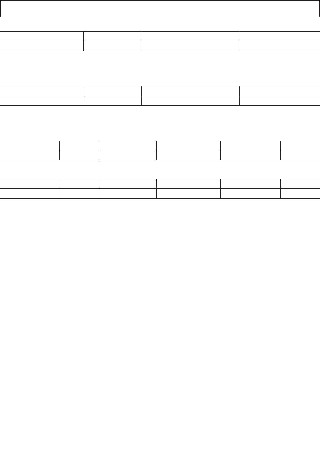
Table XVI. Data Capture Register Write Format
Byte 0 Byte 1 Byte 2 Byte 3
00000, R/Wb, Adr[9:8] Adr[7:0] 00000, ProgCount[8:6]
1
ProgCount[5:0], RegSel[1:0]
1, 2
NOTES
1. ProgCount[8:0] = value of program counter where trap occurs (see Table XXI).
2. RegSel[1:0] selects one of four registers (see Data Capture Register section).
Table XVII. Data_Capture_Serial Out Register (Address and Register Select) Write Format
Byte 0 Byte 1 Byte 2 Byte 3
00000, R/Wb, Adr[9:8] Adr[7:0] 00000, ProgCount[8:6]
1
ProgCount[5:0], RegSel[1:0]
1, 2
NOTES
1. ProgCount[8:0] = value of program counter where trap occurs (see Table XXI).
2. RegSel[1:0] selects one of four registers (see Data Capture Registers section).
Table XVIII. Data Capture Read Format
Byte 0 Byte 1 Byte 2 Byte 3 Byte 4 Byte 5
00000, R/Wb, Adr[9:8] Adr[7:0] 00000000 Data[23:16] Data[15:8] Data[7:0]
Table XIX. Safeload Register Write Format
Byte 0 Byte 1 Byte 2 Byte 3 Byte 4 Byte 5
00000, R/Wb, Adr[9:8] Adr[7:0] ParamAdr[7:0] 00, Param[21:16] Param[15:8] Param[7:0]
INITIALIZATION
Power-Up Sequence
The AD1953 has a built-in power-up sequence that initializes
the contents of all internal RAMs. During this time, the contents
of the internal program boot ROM are copied to the internal
program RAM, and likewise the SPI parameter RAM is filled
with values from its associated boot ROM. The data memories
are also cleared during this time.
The boot sequence lasts for 1024 MCLK cycles and starts on
the rising edge of the RESETB pin. Since the boot sequence
requires a stable master clock, the user should avoid writing to
or reading from the SPI registers during this period of time.
Note that the default power-on state of the internal clock mode
circuitry is 512 × f
S
, or about 24 MHz for normal audio sample
rates. This mode bypasses all the internal clock doublers and
allows the external master clock to directly operate the DSP
core. If the external master clock is 256 × f
S
, the boot sequence will
operate at this reduced clock rate and take slightly longer to
complete. After the boot sequence has finished, the clock modes
may be set via the SPI port. For example, if the external master
clock frequency is 256 × f
S
clock, the boot sequence would
take 1024 256 × f
S
clock cycles to complete, after which an
SPI write could occur to put the AD1953 in 256 × f
S
mode.
The default state of the MCLK input selector is MCLK0. Since
this input selector is controlled using the SPI port, and the SPI
port cannot be written to until the boot sequence is complete,
there must be a stable master clock signal present on the MCLK0
pin at startup.
Setting the Clock Mode
The AD1953 contains a clock doubler circuit that is used to
generate an internal 512 × f
S
clock when the external clock is
256 × f
S
. The clock mode is set by writing to Bit <2> of Control
Register 2.
When the clock mode is changed, it is possible that a glitch will
occur on the internal MCLK signal. This may cause the proces-
sor to inadvertently write an incorrect value into the data RAM,
which could cause an audio pop or click sound. To prevent this,
it is recommended that the following procedure be followed:
1. Assert the soft power-down bit (Bit <6> in Control Register 1)
to stop the internal MCLK.
2. Write the desired clock mode into Bit <2> of Control Register 2.
3. Wait at least 1 ms while the clock doublers settle.
4. Deassert the soft power-down bit.
An alternative procedure is to initiate a soft shutdown of the
processor core by writing a 1 to the halt program bit in Control
Register 1. This initiates a volume ramp-down sequence followed
by a shutdown of the DSP core. Once the core is shut down
(which can be verified by reading Bit <1> from Control Register 1,
or by waiting at least 20 ms), the new clock mode can be
programmed by writing to Bit <2> of Control Register 2. The
DSP core can then be restarted by clearing the halt program bit
in Control Register 1.
REV. A
AD1953
–28–
Setting the Data and MCLK Input Selectors
The AD1953 contains input selectors for both the serial data
inputs as well as the MCLK input. This allows the AD1953 to
select a variety of input and clock sources with no external hard-
ware required. These input selectors are controlled by writing to
SPI Control Register 2.
When the DATA source or MCLK source is changed by writing
to the SPI port, it is possible that a pop or click will occur in the
audio. To prevent this noise, the core should be shut down by
writing a 1 to the “halt program” bit in Control Register 1. This
initiates a volume ramp-down sequence followed by a shutdown
of the DSP core. Once the core is shut down (which can be
verified by reading Bit <1> from Control Register 1, or by wait-
ing at least 20 ms after the halt program command is issued),
the new DATA or MCLK source can be programmed by writ-
ing to Control Register 2. The DSP core can then be restarted
by clearing the “halt-program” bit in Control Register 1.
DATA CAPTURE REGISTERS AND OUTPUTS
The AD1953 incorporates a feature called “data capture.” Using
this feature, any node in the signal processing flow may be sent
either to an SPI-readable register, to a dedicated serial output
pin (2-channel output), or to a set of dual-function pins (6-channel
TDM mode). This allows the basic functionality of the AD1953
to be extended to a larger number of channels, or alternatively it
can be used to monitor and display information about signal
levels or compressor/limiter activity.
The AD1953 contains eight independent data capture registers.
The Data Capture SPI Out registers are used for reading back
internal DSP signals over the SPI port. These registers can be
used for a variety of purposes. One example might be to access
the dB output of the internal rms detector, to run a front-panel
signal level display.
The remaining data capture registers are used to output internal
DSP signals to external DACs, CODECs, or DSP chips. There
are two possible output modes, detailed in the following table.
Table XX. Data Capture/TDM Mode Settings
DMUXO/TDMO,
Control DCSOUT LRMUXO/TDMFS,
Reg 1, Bits Control Reg Pin (45) BMUXO/TDMBC
<13:12> 2, Bit <8> Functions Pin Functions
00 0 OFF OFF
00 1 OFF Serial MUX Output
01 Don’t care OFF TDM Data Capture
Outputs and Clocks,
6-channel Output
10 0 ON, 2- OFF
channel
output.
10 1 ON, 2- Serial MUX Output
channel
output.
In TDM output mode, the Serial Mux Out multifunction pins
(41–43) are used to output 6-channel TDM data, BCLK, and
frame sync signals. In 2-channel output mode, the data appears
on Pin 45, and can be used with the BCLK and LRCLK signals
that are already present on the serial input pins. The data will
be formatted in the same way as the input data. The data cap-
ture feature is primarily intended to feed signals to external
DACs, DSPs, or CODECs, such as the AD1836, in order to
extend the number of channels that the internal DSP can access.
For each of the data capture registers, a capture count and a
register select must be set. The capture count is a number between
0 and 511 that corresponds to the program step number where
the capture will occur. The register-select field programs one of
four registers in the DSP core that will be transferred to the data
capture register when the program counter equals the capture
count. The register select field is decoded as follows:
00: Multiplier Output (Mult_Out)
01: Output of dB conversion block (DB_OUT)
10: Multiplier Data Input (MDI)
11: Multiplier Coefficient Input (MCI)
The capture count and register select bits are set by writing to
one of the four data capture registers at the following SPI addresses:
266: SPI data capture setup register 1
267: SPI data capture setup register 2
268: Data Capture serial out setup register 0
269: Data Capture serial out setup register 1
270: Data Capture serial out setup register 2
271: Data Capture serial out setup register 3
272: Data Capture serial out setup register 4
273: Data Capture serial out setup register 5
The format of the captured data varies according to the register
select fields. Data captured from the Mult_Out setting is in 1.23
twos complement format, so that a full-scale input signal will
produce a full-scale digital output (assuming no processing). If
the parameters are set such that the input-to-output gain is
more than 0 dB, then the digital output will be clipped.
Data captured from the DB_OUT setting is in 5.19 format,
where the actual rms dB level is equal to –87 + (3 × DB_OUT).
In this equation, DB_OUT is the value that is captured. It
follows that in this data format, the actual output readings will
range from –87 dB to +9 dB. The AD1953 uses the convention
that 0 dB is the rms value of the full-scale digital signal.
Data captured using the MDI setting is in 3.21 format. A 0 dB
digital input will produce a –12 dB digital output, assuming the
AD1953 is set for no processing.
Data captured using the MCI setting is in 2.20 format. This data
is generally a signal gain or filter coefficient, and therefore it does
not make sense to talk about the input-to-output gain. A coeffi-
cient of 0100000000000000000000 corresponds to a gain of 1.0.
The data that must be written to set up the data capture is a
concatenation of the 9-bit program count index with the 2-bit
register select field.
The SPI capture registers can be accessed by reading from SPI
locations 266 (for SPI capture register 1) or 267 (for SPI capture
register 2). The other six data capture registers (data capture
serial-out) automatically transfer their data to either the Data
Capture Serial Out (DCSOUT) pin in 2-channel mode or the
DMUXO/TDMO pin in TDM mode. In 2-channel mode,
DCSOUT capture register 1 is present in the left data slot (as
defined by the serial input format) and DCSOUT capture regis-
ter 2 is present in the right data slot.
REV. A
AD1953
–29–
Table XXI. Data Capture Trap Indexes and Register Select
Program Count
Signal Description Index (9 Bits) Register Select (2 Bits) Numeric Format
HPF Out Left 15 Mult_Out 1.23, Clipped
HPF Out Right 259 Mult_Out 1.23, Clipped
De-emphasis Out Left 19 Mult_Out 1.23, Clipped
De-emphasis Out Right 263 Mult_Out 1.23, Clipped
Left Biquad 0 Output 34 Mult_Out 1.23, Clipped
Left Biquad 1 Output 43 Mult_Out 1.23, Clipped
Left Biquad 2 Output 52 Mult_Out 1.23, Clipped
Left Biquad 3 Output 61 Mult_Out 1.23, Clipped
Left Biquad 4 Output 70 Mult_Out 1.23, Clipped
Left Biquad 5 Output 79 Mult_Out 1.23, Clipped
Left Biquad 6 Output 88 Mult_Out 1.23, Clipped
Right Biquad 0 Output 284 Mult_Out 1.23, Clipped
Right Biquad 1 Output 293 Mult_Out 1.23, Clipped
Right Biquad 2 Output 302 Mult_Out 1.23, Clipped
Right Biquad 3 Output 311 Mult_Out 1.23, Clipped
Right Biquad 4 Output 320 Mult_Out 1.23, Clipped
Right Biquad 5 Output 329 Mult_Out 1.23, Clipped
Right Biquad 6 Output 338 Mult_Out 1.23, Clipped
Volume Out Left 114 Mult_Out 1.23, Clipped
Volume Out Right 111 Mult_Out 1.23, Clipped
Volume Out Sub 459 Mult_Out 1.23, Clipped
Phat Stereo Out Left 115 Mult_Out 1.23, Clipped
Phat Stereo Out Right 112 Mult_Out 1.23, Clipped
Delay Output Left 190 Mult_Out 1.23, Clipped
Delay Output Right 361 Mult_Out 1.23, Clipped
Main Compressor rms Out (dB)
154 DB_Out 24-Bit Positive Binary, Bit <19>
Corresponds to a 3 dB Change
Main Compressor Gain Reduction 165 MCI 2.22, 2 LSB = 0
(Linear)
Look-Ahead Delay Output Left 165 MDI 3.21, 2 LSBs truncated
Look-Ahead Delay Output Right 178 MDI 3.21, 2 LSBs truncated
Main Compressor Out Left 175 Mult_Out 1.23, Clipped
Main Compressor Out Right 188 Mult_Out 1.23, Clipped
Interpolator Input Left 191 Mult_Out 1.23, Clipped
(includes SUB Reinject)
Interpolator Input Right 362 Mult_Out 1.23, Clipped
(includes SUB Reinject)
Sub Channel Filter Input 430 Mult_Out 1.23, Clipped
Sub XOVER Biquad 0 Output 438 Mult_Out 1.23, Clipped
Sub XOVER Biquad 1 Output 447 Mult_Out 1.23, Clipped
Sub XOVER Biquad 2 Output 456 Mult_Out 1.23, Clipped
Left XOVER Biquad 0 Output 99 Mult_Out 1.23, Clipped
Left XOVER Biquad 1 Output 108 Mult_Out 1.23, Clipped
Right XOVER Biquad 0 Output 349 Mult_Out 1.23, Clipped
Right XOVER Biquad 1 Output 358 Mult_Out 1.23, Clipped
Sub Delay Output 511 Mult_Out 1.23, Clipped
Sub rms Biquad Output 467 Mult_Out 1.23, Clipped
Sub rms Output (dB) 489 DB_Out
24-Bit Positive Binary, Bit <19>
Corresponds to a 3 dB Change
Sub Compressor Gain (Linear) 495 MCI 2.22, 2 LSB = 0
Sub Channel Output 511 Mult_Out 1.23, Clipped
REV. A

AD1953YSTZRL

Mfr. #:
Manufacturer:
Analog Devices Inc.
Description:
Audio DSPs IC Digital Audio Processor
Lifecycle:
New from this manufacturer.
Delivery:
DHL FedEx Ups TNT EMS
Payment:
T/T Paypal Visa MoneyGram Western Union

Products related to this Datasheet