–3–
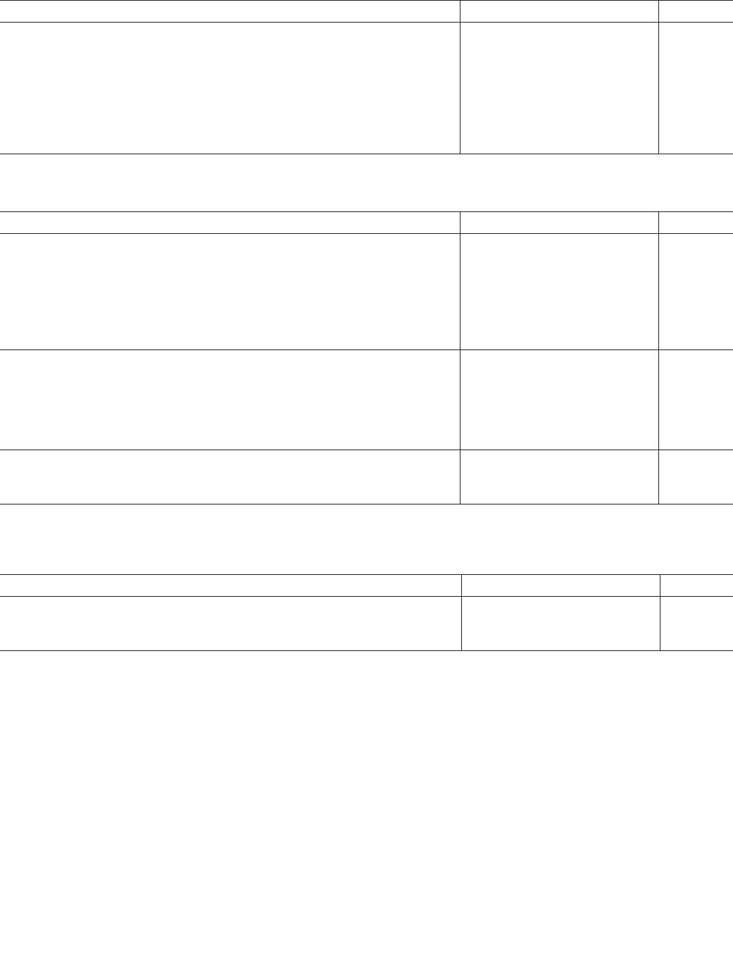
TEST CONDITIONS, UNLESS OTHERWISE NOTED.
Supply Voltages (AVDD, DVDD) 5.0 V
Ambient Temperature 25°C
Input Clock 12.288 MHz
Input Signal 1.000 kHz 0 dB Full Scale
Input Sample Rate 48 kHz
Measurement Bandwidth 20 Hz to 20 kHz
Word Width 24 Bits
Load Capacitance 2200 pF
Load Impedance 2.74 kΩ
Input Voltage High 2.1 V
Input Voltage Low 0.8 V
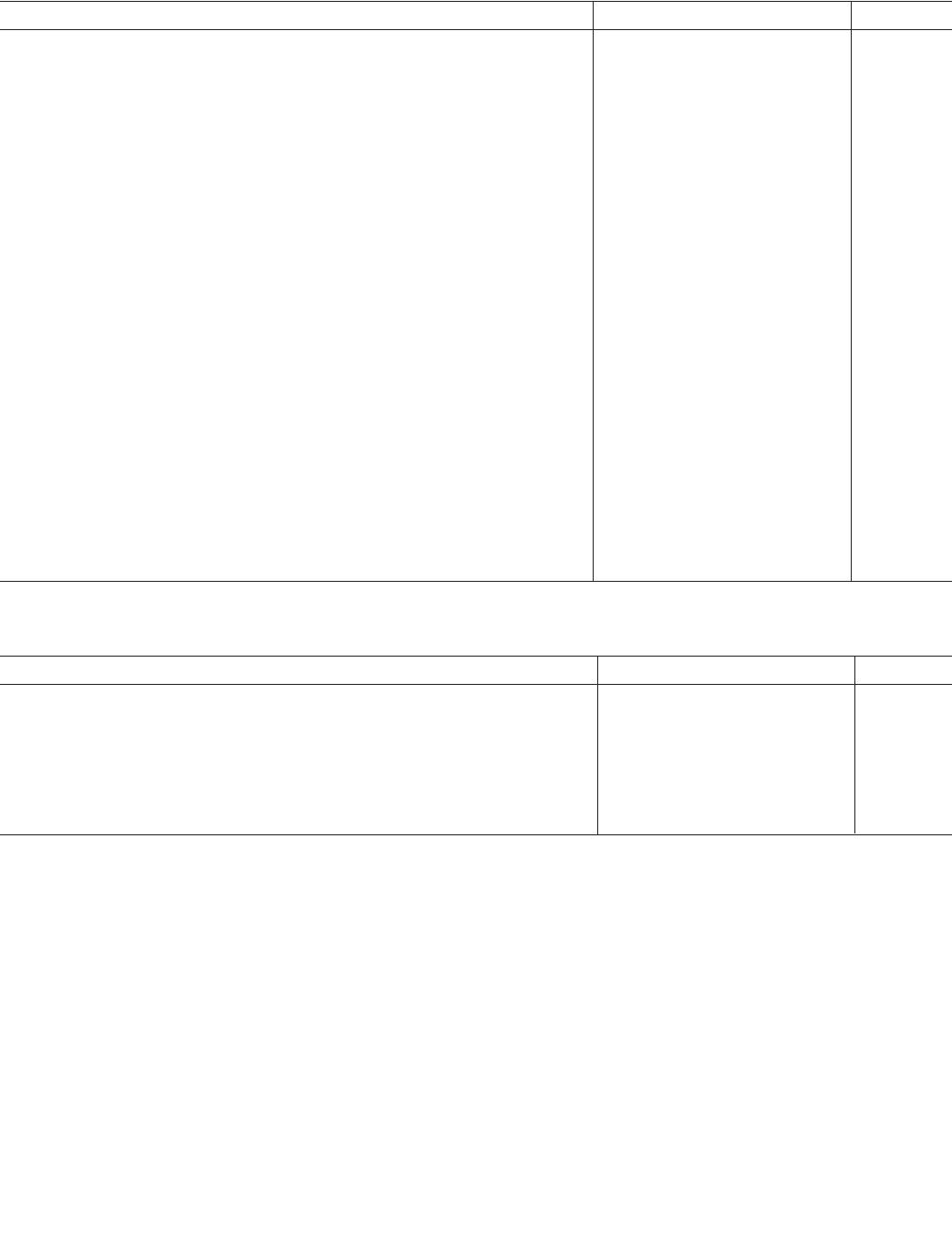
ANALOG PERFORMANCE*
Parameter Min Typ Max Unit
RESOLUTION 24 Bits
SIGNAL-TO-NOISE RATIO (20 Hz to 20 kHz) (Left/Right Output)
No Filter (Stereo) 109 dB
With A-Weighted Filter 112 dB
DYNAMIC RANGE (20 Hz to 20 kHz, –60 dB Input) (Left/Right Output)
No Filter 109 dB
With A-Weighted Filter 108 112 dB
TOTAL HARMONIC DISTORTION PLUS NOISE (Left/Right Output)
V
O
= –0.5 dB –93 –100 dB
SIGNAL-TO-NOISE RATIO (20 Hz to 20 kHz) (Subwoofer Output)
No Filter (Stereo) 104 dB
With A-Weighted Filter 107 dB
DYNAMIC RANGE (20 Hz to 20 kHz, –60 dB Input) (Subwoofer Output)
No Filter 104 dB
With A-Weighted Filter 104 107 dB
TOTAL HARMONIC DISTORTION PLUS NOISE (Subwoofer Output)
V
O
= –0.5 dB –90 –96 dB
ANALOG OUTPUTS
Differential Output Range (± Full Scale) (Left/Right Output) 2.72 V p-p
Differential Output Range (± Full Scale) (Subwoofer Output) 2.79 V p-p
CMOUT 2.50 V
DC ACCURACY
Gain Error (Left/Right Channel) –5 +5 %
Gain Error (Subwoofer Channel) –8 +8 %
Interchannel Gain Mismatch –0.250 +0.250 dB
Gain Drift 150 ppm/°C
DC Offset –35 +35 mV
INTERCHANNEL CROSSTALK (EIAJ Method) –120 dB
INTERCHANNEL PHASE DEVIATION ±0.1 Degrees
MUTE ATTENUATION –107 dB
DE-EMPHASIS GAIN ERROR ±0.1 dB
*Performance of right and left channels is identical (exclusive of the Interchannel Gain Mismatch and Interchannel Phase Deviation specifications).
Specifications subject to change without notice.
SPECIFICATIONS
AD1953
REV. A
AD1953
–4–
DIGITAL I/O
Parameter Min Typ Max Unit
Input Voltage High (V
IH
) 2.1 V
Input Voltage High (V
IH
) – RESETB 2.25 V
Input Voltage Low (V
IL
) 0.8 V
Input Leakage (I
IH
@ V
IH
= 2.1 V) 10 μA
Input Leakage (I
IL
@ V
IL
= 0.8 V) 10 μA
High Level Output Voltage (V
OH
), I
OH
= 2 mA DVDD – 0.5 V
Low Level Output Voltage (V
OL
), I
OL
= 2 mA 0.4 V
Input Capacitance 20 pF
Specifications subject to change without notice.
POWER
Parameter Min Typ Max Unit
SUPPLIES*
Voltage: Analog, and Digital 4.5 5 5.5 V
Analog Current 42 48 mA
Analog Current, Power-Down 40 46 mA
Digital Current 66 76 mA
Digital Current, SPI Power-Down 6 10 mA
Digital Current, Reset Power-Down 54 62 mA
DISSIPATION
Operation, Both Supplies 540 mW
Operation, Analog Supplies 210 mW
Operation, Digital Supplies 330 mW
SPI Power-Down, Both Supplies 230 mW
Reset Power-Down, Both Supplies 470 mW
POWER SUPPLY REJECTION RATIO
1 kHz 300 mV p-p Signal at Analog Supply Pins –80 dB
20 kHz 300 mV p-p Signal at Analog Supply Pins –80 dB
*ODVDD current is dependent on load capacitance and clock rate.
Specifications subject to change without notice.
TEMPERATURE RANGE
Parameter Min Typ Max Unit
Specifications Guaranteed 25 °C
Functionality Guaranteed –40 105 °C
Storage –55 125 °C
Specifications subject to change without notice.
REV. A
–5–
AD1953
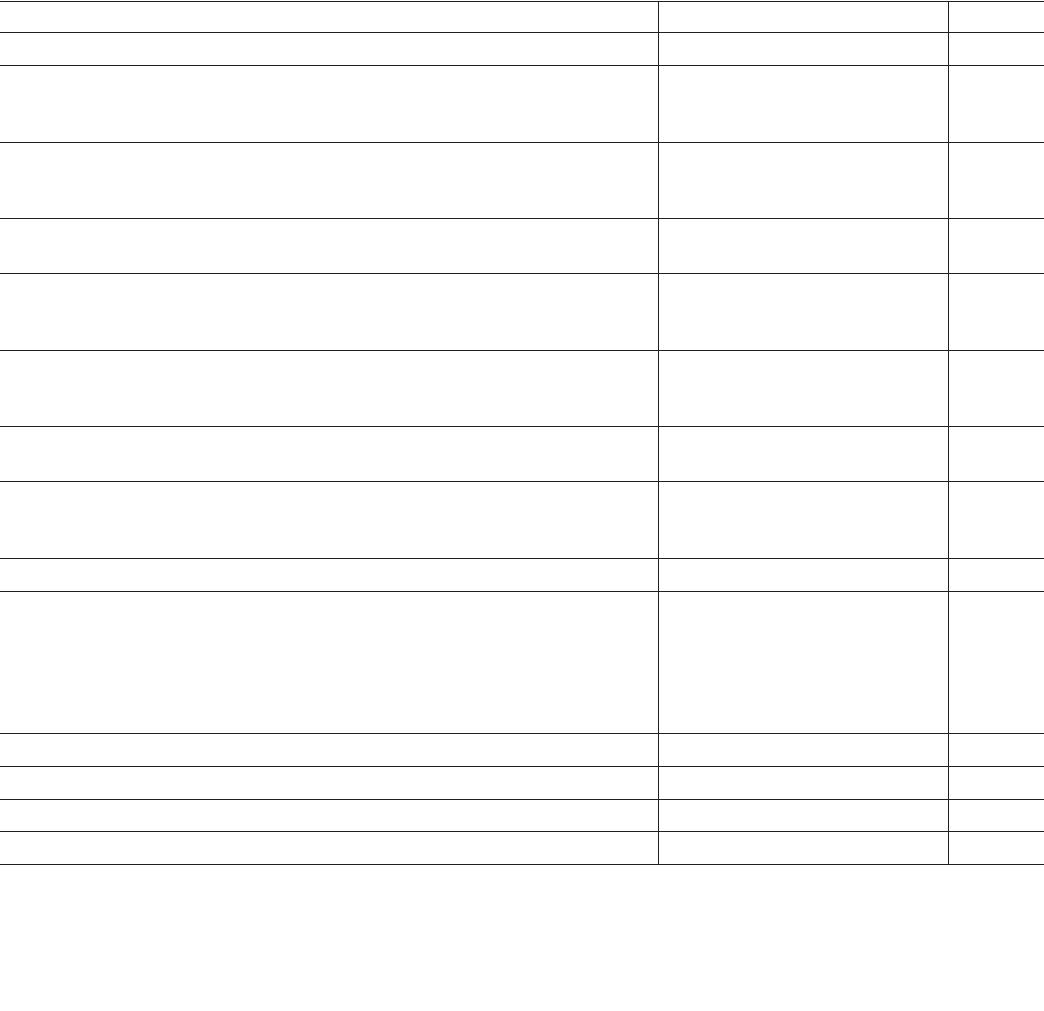
DIGITAL TIMING
Parameter Min Typ Max Unit
t
DMD
MCLK Recommended Duty Cycle @ 12.288 MHz (256 f
S
Mode) 45 55 %
t
DMD
MCLK Recommended Duty Cycle @ 24.576 MHz (512 f
S
Mode) 40 60 %
t
DMD
MCLK Delay (All Mode) 25 ns
t
DBH
BCLK Low Pulsewidth 10 ns
t
DBH
BCLK High Pulsewidth 10 ns
t
DBD
BCLK Delay (to BCLKO) 25 ns
t
DLS
LRCLK Setup 0 ns
t
DLH
LRCLK Hold 10 ns
t
DLD
LRCLK Delay (to LRCLKO) 25 ns
t
DDS
SDATA Setup 0 ns
t
DDH
SDATA Hold 10 ns
t
DDD
SDATA Delay (to SDATAO) 25 ns
t
TFS
TDMFS Delay (from MCLK) 35 ns
t
TBS
TDMBC Delay (from MCLK) 35 ns
t
TOS
TDMO Delay (from TDMBC) 5 ns
t
CCL
CCLK Low Pulsewidth 12 ns
t
CCH
CCLK High Pulsewidth 12 ns
t
CLS
CLATCH Setup 10 ns
t
CLH
CLATCH Hold 10 ns
t
CLD
CLATCH High Pulsewidth 10 ns
t
CDS
CDATA Setup 0 ns
t
CDH
CDATA Hold 10 ns
t
COD
COUT Delay 35 ns
t
COH
COUT Hold 2 ns
t
DCD
DCSOUT Delay 35 ns
t
DCH
DCSOUT Hold 2 ns
t
PDRP
PD/RST Low Pulsewidth 5 ns
Specifications subject to change without notice.
DIGITAL FILTER CHARACTERISTICS at 44.1 kHz
Parameter Min Typ Max Unit
Pass-Band Ripple ±0.01 dB
Stop-Band Attenuation 70 dB
Pass Band 20 kHz
0.4535 f
S
Stop Band 24 kHz
0.5442 f
S
Group Delay 24.625/f
S
sec
Specifications subject to change without notice.
REV. A

AD1953YSTZRL

Mfr. #:
Manufacturer:
Analog Devices Inc.
Description:
Audio DSPs IC Digital Audio Processor
Lifecycle:
New from this manufacturer.
Delivery:
DHL FedEx Ups TNT EMS
Payment:
T/T Paypal Visa MoneyGram Western Union

Products related to this Datasheet