EXAR Corporation, 48720 Kato Road, Fremont, CA 94538 • (510) 668-7000 • FAX (510) 668-7017 • www.exar.com
XRD98L23
8-Bit, High-speed Linear CIS/CCD Sensor
Signal Processor with Serial Control
November 2002-2
FEATURES
· 8-Bit Resolution, No Missing Codes
· One-channel 10MSPS Pixel Rate
· Dual-channel 5MSPS Pixel Rate
· Three-channel 3 MSPS Pixel Rate
· 6-bit Programmable Gain Amplifier
· 8-bit Programmable Offset Adjustment
· CIS or CCD Compatibility
· Internal Clamp for CIS or CCD AC Coupled
Configurations
· 3.3V Operation & I/O Compatibility
· Serial Load Control Registers
· Low Power CMOS: 75mW-typ
· Low Cost 20-Lead Packages
· USB Compliant
APPLICATIONS
· Check Scanners
· General Purpose CIS or CCD Imaging
· Low Cost Data Acquisition
· Simple and Direct Interface to Canon 600 DPI
Sensors
ORDERING INFORMATION
Package Type Temperature Range Part Number
20-Lead SOIC 0°C to +70°C XRD98L23ACD
20-Lead SSOP 0°C to +70°C XRD98L23ACU
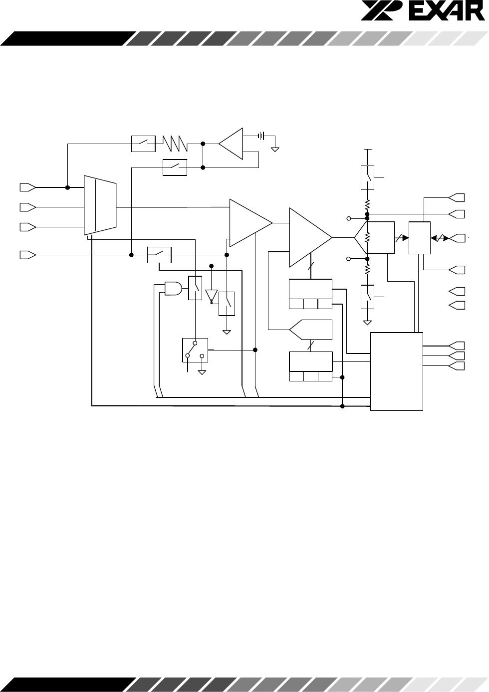
GENERAL DESCRIPTION
The XRD98L23 is a complete linear CIS or CCD sensor
signal processor on a single monolithic chip. The
XRD98L23 includes a high speed 8-bit resolution ADC,
a 6-bit Programmable Gain Amplifier with gain adjust-
ment of 1 to 10, and a typical 8-bit programmable input
referred offset calibration range of 480mV.
In the CCD configuration the input signal is AC coupled
with an external capacitor. An internal clamp sets the
black level. In the CIS configuration, the clamp switch
can be disabled and the CIS output signal is DC
coupled from the CIS sensor to the XRD98L23. The
CIS signal is level shifted to VRB in order to use the full
range of the ADC. In the CIS configuration the input can
also be AC coupled similar to the CCD configuration.
This enables CIS signals with large black levels to be
internally clamped to a DC reference equal to the black
level. The DC reference is internally subtracted from
the input signal.
The CIS configuration can also be used in other
applications that do not require CDS function, such as
low cost data acquisition.
Rev. 1.00