XRD98L23
19
Rev. 1.00
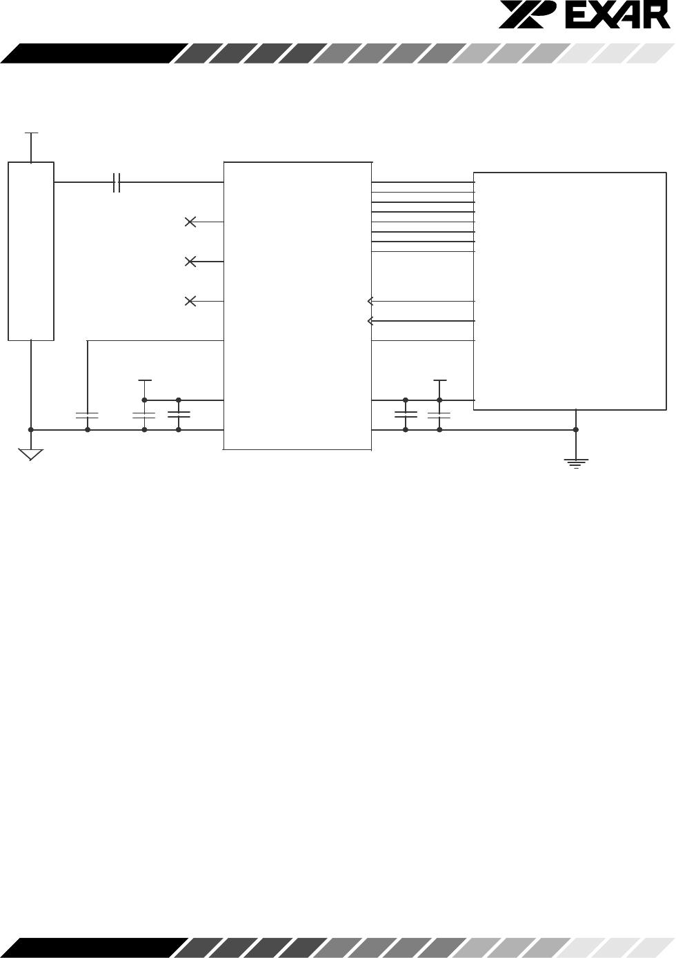
Area or Linear CCD Applications
Figure 13, is a block diagram for applications with Area
or Linear CCDs (The timing for Area CCDs and B/W
CCDs is the same). For Area or Linear CCD applica-
tions, a global offset is loaded into the serial port at the
beginning of a line. The gain is set to adjust for the
highest color intensity of the CCD output. Once the
pixel values have been sampled, the gain and offset are
adjusted at the beginning of the next line. For example,
if there is a line-to-line variation between the black
reference pixels, the offset is adjusted. The gain is
always adjusted for the highest color intensity.
Figure 13. CCD AC Coupled Application
RL
VRT
VRB
VDD
RED
XRD98L23
CLAMP
M
U
X
AREA
or
LINEAR
CCD
N/C
N/C
N/C
XRD98L23
20
Rev. 1.00
Figure 14. Typical Application Circuitry for a Single
Channel B/W CCD AC Coupled Inverted Mode
DVDD (3V)
AVDD
VCC (5V - 15V)
DGND
AGND
DIGITAL
ASIC
C
C
D
N/C
N/C
N/C
100PF
0.1uF
0.1uF
0.01uF
0.1uF
0.01uF
XRD98L23
DVDD
1
DB0
2
DB1
3
DB2
4
DB3
5
DB4
6
DB5/SCLK
7
DB6/SDATA
8
DB7/LD
9
DGND
10
ADCCLK
11
CLAMP
12
SYNCH
13
AGND
14
VREF+
15
VDCEXT
16
BLU
17
GRN
18
RED
19
AVDD
20
XRD98L23
21
Rev. 1.00
tdv tdv
AREA, LINEAR or B/W CCD -- AC Coupled
(CLAMP Enabled)
Pixel N-1 Pixel N Pixel N+1
CCD
Channel N
ADCCLK
tckpd
tap
tap
tckhw tcklw
CLAMP
tclpw
N-8
N/A N-7
N/A
N-6
N.A
[7:0]
DB
Figure 15. Timing Diagram for Figure 14
Triple Channel CCD Application
Figure 16, is a block diagram for pixel-by-pixel applica-
tions with triple channel CCDs. During the optically
shielded section of a pixel, CLAMP must go high to
store the black reference on each capacitor to the input.
The gain and offset is automatically rotated to adjust for
each channel input. The data is available on the output
bus on the falling edge of ADCCLK.

XRD98L23ACU

Mfr. #:
Manufacturer:
MaxLinear
Description:
Analog Front End - AFE
Lifecycle:
New from this manufacturer.
Delivery:
DHL FedEx Ups TNT EMS
Payment:
T/T Paypal Visa MoneyGram Western Union

Products related to this Datasheet