Expand menu
Hello, Sign in
My Account
0
Cart
Home
Products
Sensors
Semiconductors
Passive Components
Connectors
Power
Electromechanical
Optoelectronics
Circuit Protection
Integrated Circuits - ICs
Main Products
Manufacturers
Blog
Services
About OMO
About Us
Contact Us
Check Stock
XRD98L23ACU
P1-P3
P4-P6
P7-P9
P10-P12
P13-P15
P16-P18
P19-P21
P22-P24
P25-P27
P28-P30
P31-P32
XRD98L23
10
Rev. 1.00
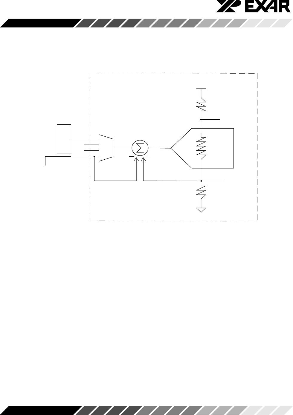
RL
VRT
VRB
VDD
RED
XRD98L23
DC
REFERENCE
C
I
S
M
U
X
N/C
N/C
VDCEXT
The DC reference voltage applied to VDCEXT does not
have to be accurate. The internal offset DAC voltage is
still used in this mode for fine adjustment. VDCEXT
cannot be used as an input from the CIS. Any signal
applied to VDCEXT will be subtracted from the output
signal of the multiplexer.
Figure 4. Application with Offset Greater Than (-60mv to 300mv)
XRD98L23
11
Rev. 1.00
AGND
DVDD (3V)
VCC (5V - 15V)
AVDD
DGND
AVDD
ASIC
DIGITAL
C
I
S
N/C
N/C
4
K
0.
1uF
0.
01uF
0.1uF
0.
01uF
0.
1uF
0.1
uF
1
K
XRD98L23
DVDD
1
DB0
2
DB1
3
DB2
4
DB3
5
DB4
6
DB5/SCLK
7
DB6/SDATA
8
DB7/LD
9
DGND
10
ADCCLK
11
CLAMP
12
SYNCH
13
AGND
14
VREF+
15
VDCEXT
16
BLU
17
GRN
18
RED
19
AVDD
20
Figure 5. Typical Application Circuitry CIS DC Coupled Non-Inverted Mode with
VDC External Offset Compensation
XRD98L23
12
Rev. 1.00
CIS Mode Timing -- DC Coupled
(CLAMP disabled)
ADCCLK
tckhw
tcklw
tckpd
tap
tap
Pixel N-1
Pixel N
tdv
Pixel N+1
CIS
tdv
[7:0]
N-8
N/A
N-7
N/A
N-6
N/A
N-5
N/A
DB
Figure 6. Timing Diagram for Figure 5
ADCCLK
Events
↓
ADC Sample & PGA Start Tracking next Pixel
Data Out
↑
Invalid Data Out
HI
ADC Track PGA Output
LO
ADC Hold/Convert
Table 1.
Mode 2. AC Coupled
If the CIS signal has a black reference for the video
signal, an external capacitor C
EXT
is used. When
CLAMP (clamp) pin is set high an internal switch allows
one side of the external capacitor to be set to ground.
It then is level shifted to correspond to the bottom ladder
reference voltage of the ADC (Figure 7).
P1-P3
P4-P6
P7-P9
P10-P12
P13-P15
P16-P18
P19-P21
P22-P24
P25-P27
P28-P30
P31-P32
XRD98L23ACU
Mfr. #:
Buy XRD98L23ACU
Manufacturer:
MaxLinear
Description:
Analog Front End - AFE
Lifecycle:
New from this manufacturer.
Delivery:
DHL
FedEx
Ups
TNT
EMS
Payment:
T/T
Paypal
Visa
MoneyGram
Western
Union
Products related to this Datasheet
XRD98L23ACU
XRD98L23ACU-F
XRD98L23ACD-F
XRD98L23ACDTR-F