XRD98L23
9
Rev. 1.00
R
L
VRT
VRB
VDD
RED
XRD98L23
C
I
S
M
U
X
N/C
N/C
N/C
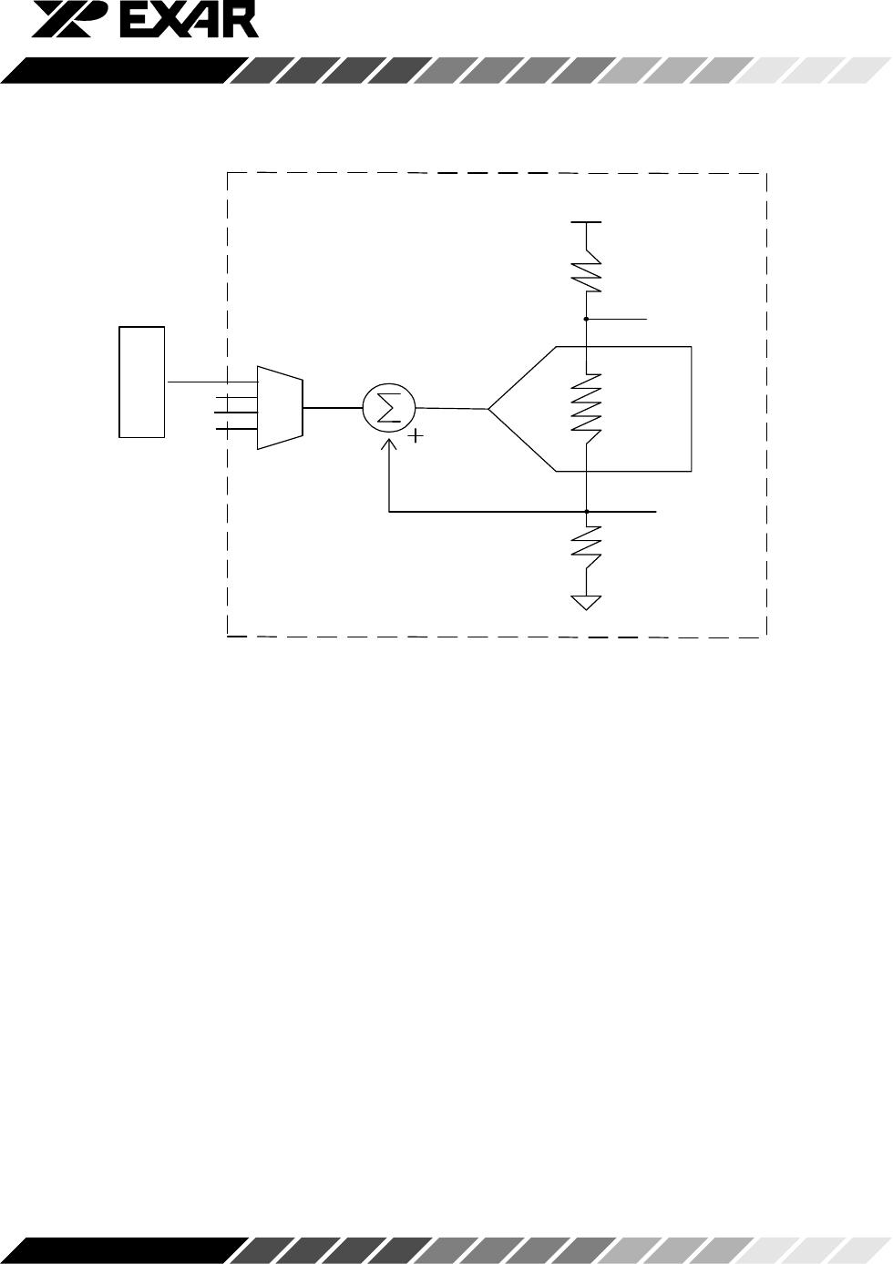
The input is added to VRB before the signal passes
through the ADC. If the CIS output is zero, then the
output of the ADC will be zero code. This enables the
CIS to be referenced to the bottom ladder reference
voltage to use the full range of the ADC.
Some CIS sensors have an output with an offset voltage
of greater than 300mV. If the CIS output is beyond the
offset range of the XRD98L23 (see Offset Control DAC,
Pg. 27) set the internal mode registers to external
reference. An external reference voltage equal to the
value of the CIS offset voltage can be applied to
VDCEXT (Figure 4) in order to meet the dynamic range
of the XRD98L23. Figure 4 is a diagram of the
XRD98L23 in the external reference mode for CIS, DC
coupled applications.
Figure 3. Application with Offset in the Range (-60mv to 300mv)