XRD98L23
18
Rev. 1.00
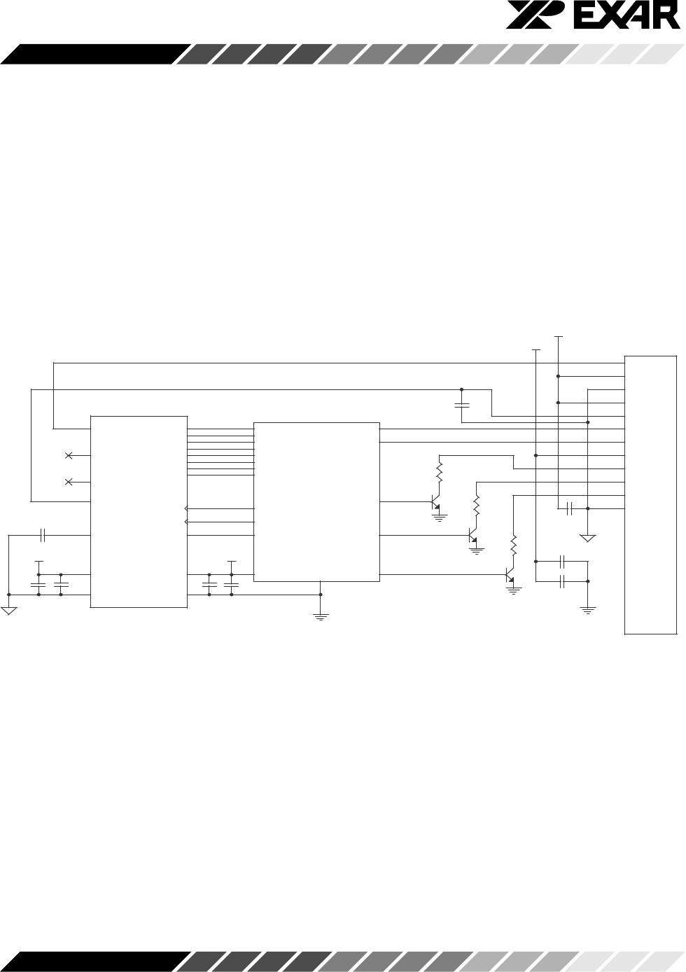
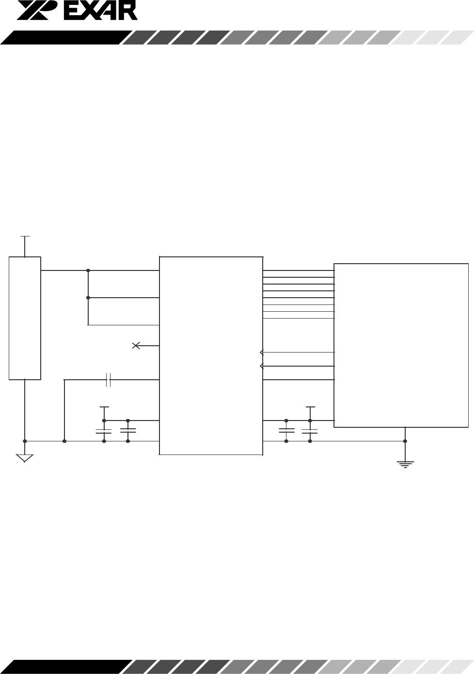
CCD Configuration (Charge Coupled Device)
Mode 1. AC Coupled
In the CCD configuration of operation, an external
capacitor needs to be chosen according to the equa-
tions below. The typical value for the external capacitor
is 100pF. This value should be adjusted according to
the time constant (Tc) needed in a particular applica-
tion. The CLAMP pin has an internal 180 ohm imped-
ance (R
INT
) which is in series with the external capacitor
(C
EXT
).
Therefore, Tc =1/R
INT
C
EXT
If the input to the external capacitor has a load imped-
ance (R
EXT
), then
T
c
=1/(R
INT
+R
EXT
)C
EXT
When CLAMP (clamp) pin is set high an internal switch
allows one side of the external capacitor to be set to
VRT (Figure 13). This value corresponds to the black
reference of the CCD. When the CLAMP pin is set back
to low, the ADC samples the video signal with respect
to the black reference. The difference between the
black reference and the video signal is the actual pixel
value of the video content. Since this value is refer-
enced to the top ladder reference voltage of the ADC a
zero input signal would yield a full scale output code.
Therefore, the output of the conversion is inverted
(internally) to correspond to zero scale output code.
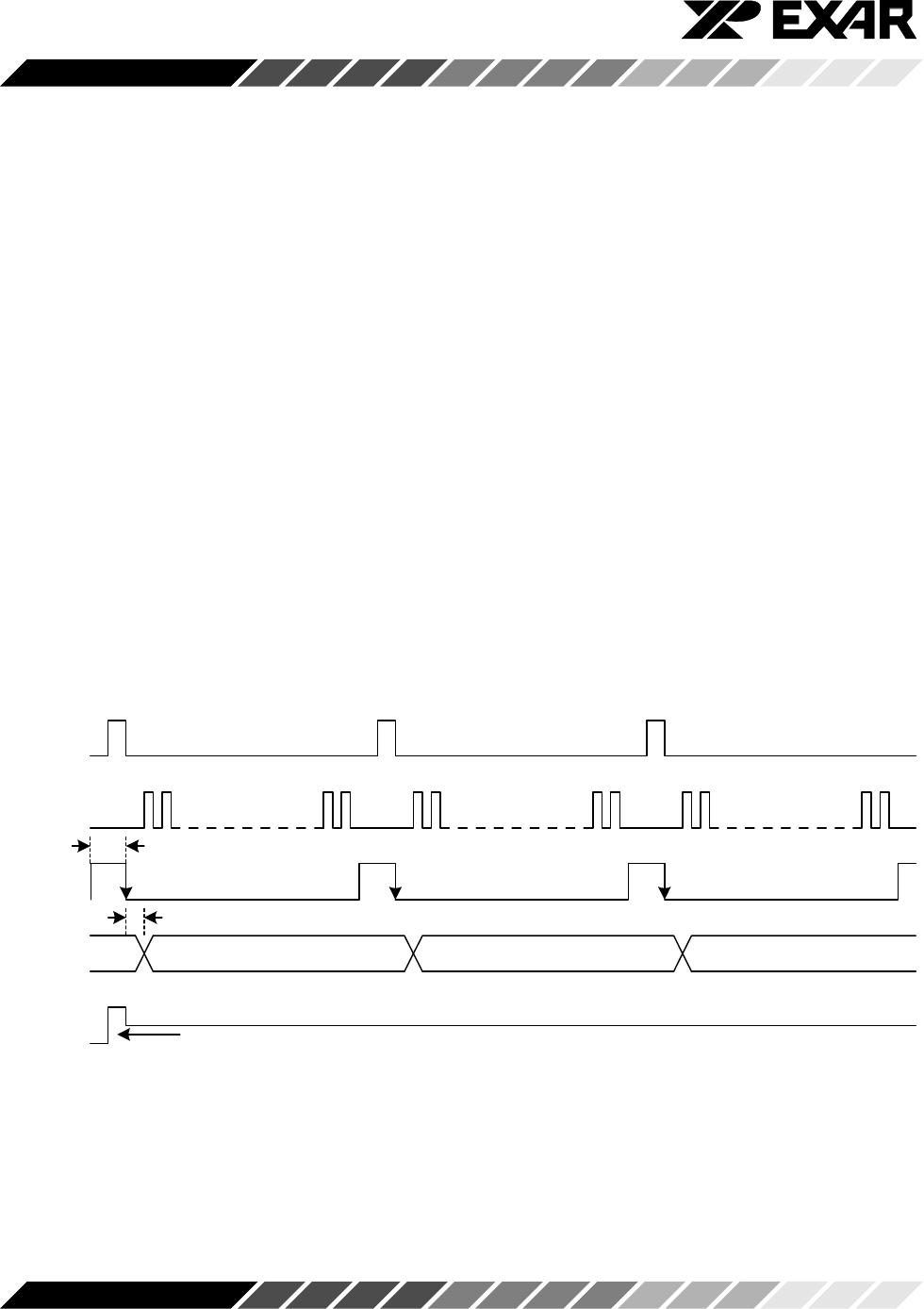
Figure 12. Timing Diagram for Figure 11
CIS Rotating Gain and Offset
Line-By-Line (Md 11)
ADCCLK
CIS
SYNCH
GAIN/
OFFSET
LD
Red Pixel Line Scan Grn Pixel Line Scan Blu Pixel Line Scan
Red Gain/Offset Cycle Grn Gain/Offset Cycle Blu Gain/Offset Cycle
Reset Internal Mux Color to Red Channel (LD = 110YYYYYY11)
tsa
tsypw
Note: Y = Previous State
Tri-State (SYNCH = LO)