XRD98L23
27
Rev. 1.00
Mode 2. DC Coupled
Typical CCDs have outputs with black references.
Therefore, DC Coupled is not recommended for CCD
applications.
Offset Control DAC
The offset DAC is controlled by 8-bits. The offset range
is 480 mV ranging from -120 mV to +300 mV (when DB5
is set to 0) and -240 mV to +240 mV (when DB5 is set
to 1). Therefore, the resolution of the 8-bit offset DAC
is 1.88 mV. However, the XRD98L23 has +/- 60 mV
reserved for internal offsets. Therefore, the effective
range for adjusting for CIS offsets or black reference is
300 mV. The offset adjustment is used primarily to
correct for the difference between the black level of the
image sensor and the bottom ladder reference voltage
(VRB) of the ADC. By adjusting the black level to
correspond to VRB, the entire range of the ADC can be
used.
If the offset of the CIS output is greater than 300 mV an
external reference can be applied to VDCEXT. The
external reference can be used to adjust for large
offsets only when the internal mode is configured
through the serial port.
Since the offset DAC adjustment is done before the
gain stage, it is gain-dependent. For example, if the
gain needs to be changed between lines (red to blue,
etc.), the offset is calibrated before the signal passes
through the PGA.
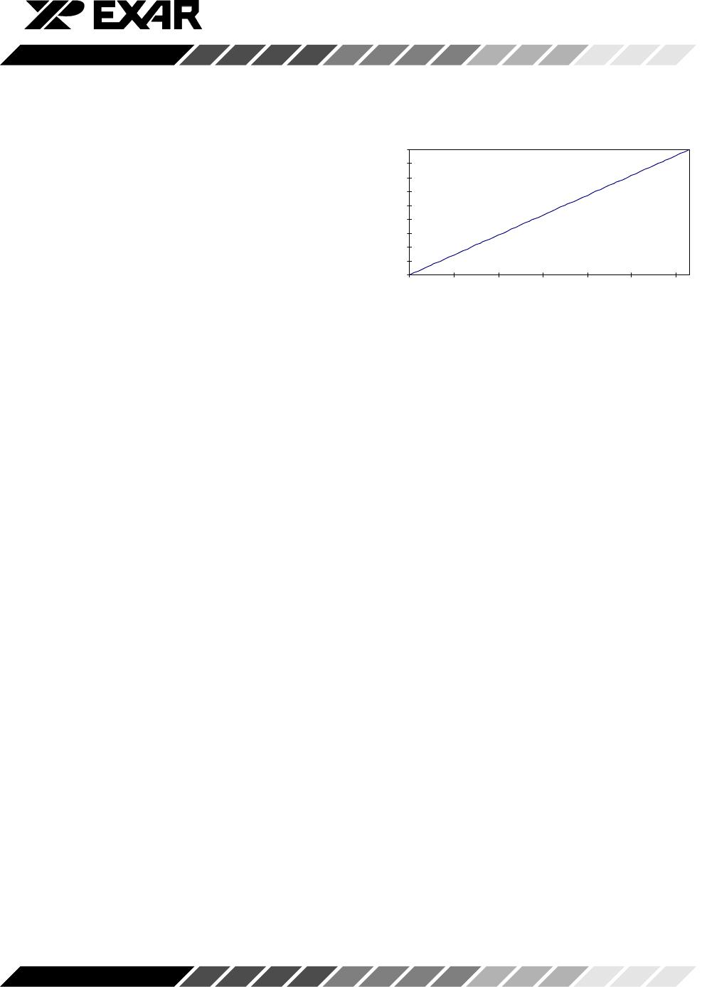
PGA (Programmable Gain Amplifier) DAC
The gain of the input waveform is controlled by a 6-Bit
PGA. The PGA is used along with the offset DAC for
the purpose of using the entire range of the ADC. The
PGA has a linear gain from 1 to 10. Figure 20, is a plot
of the transfer curve for the PGA gain.
PGA GAIN TRANSFER CURVE
GAIN 1 - 10
1
2
3
4
5
6
7
8
9
10
0 10 20 30 40 50 60
CODE
GAIN
Figure 21. Transfer Curve for the 6-Bit PGA
After the signal is level shifted to correspond with the
bottom ladder reference voltage, the system can be
calibrated such that a white video pixel can represent
the top ladder reference voltage to the ADC. This allows
for a full scale conversion maximizing the resolution of
the ADC.
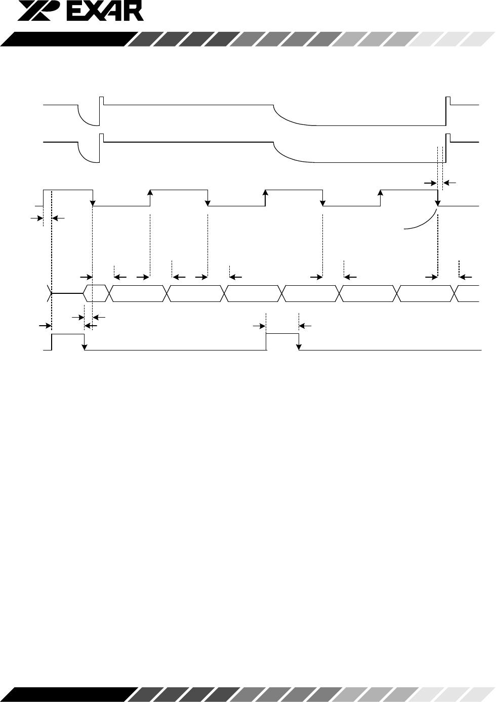
Analog to Digital Converter
The ADC is an 8-bit, 10 MSPS analog-to-digital con-
verter for high speed and high accuracy. The ADC uses
a subranging architecture to maintain low power con-
sumption at high conversion rates. The output of the
ADC is on 8-bit databus. ADCCLK samples the input
on its falling edge. After the input is sampled, the data
is latched to the output drivers. On the rising edge of
the ADCCLK, invalid data is latched to the output
drivers. There is an 8 clock cycle latency (Config 00,
11) or 6 pixel count latency (Config 01, 10) for the
analog-to-digital converter.
The V
RT
and V
RB
reference voltages for the ADC are
generated internally, unless the external V
RT
is se-
lected. In the external V
RT
mode, the V
RT
voltage is set
through the VREF+ pin. This allows the user to select
the dynamic range of the ADC.