PCA85134 All information provided in this document is subject to legal disclaimers. © NXP Semiconductors N.V. 2014. All rights reserved.
Product data sheet Rev. 2 — 6 May 2014 16 of 53
NXP Semiconductors
PCA85134
Automotive 60 x 4 LCD segment driver for low multiplex rates
7.5 Oscillator
The internal logic and the LCD drive signals of the PCA85134 are timed by the frequency
f
clk
. It equals either the built-in oscillator frequency f
osc
or the external clock frequency
f
clk(ext)
. The clock frequency f
clk
determines the LCD frame frequency (f
fr
).
7.5.1 Internal clock
The internal oscillator is enabled by connecting pin OSC to pin V
SS
. In this case, the
output from pin CLK is the clock signal for any cascaded PCA85134 in the system.
7.5.2 External clock
Pin CLK is enabled as an external clock input by connecting pin OSC to V
DD
.
Remark: A clock signal must always be supplied to the device. Removing the clock may
freeze the LCD in a DC state, which is not suitable for the liquid crystal.
7.6 Timing and frame frequency
The PCA85134 timing controls the internal data flow of the device. This includes the
transfer of display data from the display RAM to the display segment outputs. In cascaded
applications, the correct timing relationship between each PCA85134 in the system is
maintained by the synchronization signal at pin SYNC
. The timing also generates the LCD
frame signal whose frequency is derived from the clock frequency. The frame signal
frequency is a fixed division of the clock frequency from either the internal or an external
clock.
7.7 Display register
The display register holds the display data while the corresponding multiplex signals are
generated.
7.8 Segment outputs
The LCD drive section includes 60 segment outputs (S0 to S59) which should be
connected directly to the LCD. The segment output signals are generated based on the
multiplexed backplane signals and with data resident in the display register. When less
than 60 segment outputs are required, the unused segment outputs must be left
open-circuit.
Table 7. LCD frame frequencies
Operating mode ratio Frame frequency with respect to f
clk
(typical) Unit
f
clk
=1970Hz
82 Hz
f
fr
f
clk
24
--------
=
PCA85134 All information provided in this document is subject to legal disclaimers. © NXP Semiconductors N.V. 2014. All rights reserved.
Product data sheet Rev. 2 — 6 May 2014 17 of 53
NXP Semiconductors
PCA85134
Automotive 60 x 4 LCD segment driver for low multiplex rates
7.9 Backplane outputs
The LCD drive section includes four backplane outputs BP0 to BP3 which must be
connected directly to the LCD. The backplane output signals are generated in accordance
with the selected LCD drive mode.
In 1:4 multiplex drive mode: BP0 to BP3 must be connected directly to the LCD.
If less than four backplane outputs are required, the unused outputs can be left
open-circuit.
In 1:3 multiplex drive mode, BP3 carries the same signal as BP1, therefore these two
adjacent outputs can be tied together to give enhanced drive capabilities.
In 1:2 multiplex drive mode, BP0 and BP2, respectively, BP1 and BP3 carry the same
signals and can also be paired to increase the drive capabilities.
In static drive mode, the same signal is carried by all four backplane outputs and they
can be connected in parallel for very high drive requirements.
7.10 Display RAM
The display RAM is a static 60 4-bit RAM which stores LCD data. A logic 1 in the RAM
bit map indicates the on-state (V
on(RMS)
) of the corresponding LCD element. Similarly, a
logic 0 indicates the off-state (V
off(RMS)
). For more information on V
on(RMS)
and V
off(RMS)
,
see Section 7.3
.
There is a one-to-one correspondence between
the bits in the RAM bitmap and the LCD elements
the RAM columns and the segment outputs
the RAM rows and the backplane outputs.
The display RAM bit map, Figure 11
, shows row 0 to row 3 which correspond with the
backplane outputs BP0 to BP3, and column 0 to column 59 which correspond with the
segment outputs S0 to S59. In multiplexed LCD applications, the data of each row of the
display RAM is time-multiplexed with the corresponding backplane (row 0 with BP0, row 1
with BP1, and so on).
The display RAM bit map shows the direct relationship between the display RAM addresses and
the segment outputs and between the bits in a RAM word and the backplane outputs.
Fig 11. Display RAM bit map

GLVSOD\5$0DGGUHVVHVVHJPHQWRXWSXWV6
GLVSOD\5$0URZV
EDFNSODQHRXWSXWV
%3
DDD
FROXPQV
URZV
xxxxxxxxxxxxxxxxxxxxx xxxxxxxxxxxxxxxxxxxxxxxxxx xxxxxxx x x x xxxxxxxxxxxxxxxxxxxxxxxxxxxxxx xxxxxxxxxxxxxxxxxxx xx xx xxxxx
xxxxxxxxxxxxxxxxxxxxxxxxxxx xxxxxxxxxxxxxxxxxxx xxxxxx xxxxxxxxxxxxxxxxxxxxxxxxxxxxxxxxxxx xxxxxxxxxxxx x x
xxxxxxxxxxxxxxxxxxxxx xxxxxxxxxxxxxxxxxxxxxxxxxxxxxx xxxxx xxxxxxxxxxxxxxxxxxxxxxxxxxxxxxxxxxxxxxxxxxxxxxxxxx xxxxxxxx
xxxxxxxxxxxxxxxxxxxxxxxxx xxxxxxxxxxxxxxxxxxxx xxx
PCA85134 All information provided in this document is subject to legal disclaimers. © NXP Semiconductors N.V. 2014. All rights reserved.
Product data sheet Rev. 2 — 6 May 2014 18 of 53
NXP Semiconductors
PCA85134
Automotive 60 x 4 LCD segment driver for low multiplex rates
x = data bit unchanged.
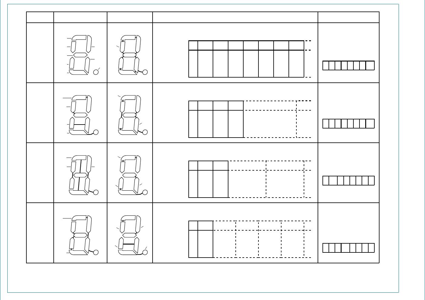
Fig 12. Relationship between LCD layout, drive mode, display RAM filling order and display data transmitted over the I
2
C-bus
DDM
DF E'3I HJG
06% /6%
E'3 F D G J I H
06% /6%
DE I JHFG'3
06% /6%
FEDI JHG'3
06% /6%
GULYHPRGH
VWDWLF

PXOWLSOH[

PXOWLSOH[

PXOWLSOH[
/&'VHJPHQWV /&'EDFNSODQHV GLVSOD\5$0ILOOLQJRUGHU WUDQVPLWWHGGLVSOD\E\WH
%3
%3
%3
%3
%3
%3
%3
%3
%3
%3
Q
F
[
[
[
E
[
[
[
D
[
[
[
I
[
[
[
J
[
[
[
H
[
[
[
G
[
[
[
'3
[
[
[
Q Q Q Q Q Q Q
URZV
GLVSOD\5$0
URZVEDFNSODQH
RXWSXWV%3
E\WH
FROXPQV
GLVSOD\5$0DGGUHVVVHJPHQWRXWSXWVV
Q
D
E
[
[
I
J
[
[
H
F
[
[
G
'3
[
[
Q Q Q
E\WH E\WH
URZV
GLVSOD\5$0
URZVEDFNSODQH
RXWSXWV%3
FROXPQV
GLVSOD\5$0DGGUHVVVHJPHQWRXWSXWVV
Q
E
'3
F
[
D
G
J
[
I
H
[
[
Q Q
E\WH E\WH E\WH
URZV
GLVSOD\5$0
URZVEDFNSODQH
RXWSXWV%3
FROXPQV
GLVSOD\5$0DGGUHVVVHJPHQWRXWSXWVV
Q
Q
D
F
E
'3
I
H
J
G
E\WH E\WH E\WH E\WH E\WH
URZV
GLVSOD\5$0
URZVEDFNSODQH
RXWSXWV%3
FROXPQV
GLVSOD\5$0DGGUHVVVHJPHQWRXWSXWVV
6
Q
6
Q
6
Q
6
Q
'3
D
I
E
J
H
F
G
6
Q
6
Q
6
Q
6
Q
6
Q
6
Q
6
Q
6
Q
'3
D
I
E
J
H
F
G
6
Q
6
Q
6
Q
'3
D
I
E
J
H
F
G
6
Q
6
Q
'3
D
I
E
J
H
F
G

PCA85134H/Q900/1,1

Mfr. #:
Manufacturer:
NXP Semiconductors
Description:
LCD Drivers 60 X 4 LCD DRIVER FOR MULTIPLEX RATES
Lifecycle:
New from this manufacturer.
Delivery:
DHL FedEx Ups TNT EMS
Payment:
T/T Paypal Visa MoneyGram Western Union

Products related to this Datasheet