PCA85134 All information provided in this document is subject to legal disclaimers. © NXP Semiconductors N.V. 2014. All rights reserved.
Product data sheet Rev. 2 — 6 May 2014 19 of 53
NXP Semiconductors
PCA85134
Automotive 60 x 4 LCD segment driver for low multiplex rates
When display data is transmitted to the PCA85134, the display bytes received are stored
in the display RAM in accordance with the selected LCD multiplex drive mode. The data is
stored as it arrives and depending on the current multiplex drive mode, data is stored
singularly, in pairs, triples, or quadruples. To illustrate the filling order, an example of a
7-segment display showing all drive modes is given in Figure 12
. The RAM filling
organization depicted applies equally to other LCD types.
The following applies to Figure 12
:
In static drive mode the eight transmitted data bits are placed into row 0 as one byte.
In 1:2 multiplex drive mode the eight transmitted data bits are placed in pairs into
row 0 and row 1 as four successive 2-bit RAM words.
In 1:3 multiplex drive mode the eight bits are placed in triples into row 0, row
1, and row 2 as three successive 3-bit RAM words, with bit 3 of the third address left
unchanged. It is not recommended to use this bit in a display because of the difficult
addressing. This last bit may, if necessary, be controlled by an additional transfer to
this address. But care should be taken to avoid overwriting adjacent data because
always full bytes are transmitted (see Section 7.10.3
).
In 1:4 multiplex drive mode, the eight transmitted data bits are placed in quadruples
into row 0, row 1, row 2, and row 3 as two successive 4-bit RAM words.
7.10.1 Data pointer
The addressing mechanism for the display RAM is realized using the data pointer. This
allows the loading of an individual display data byte, or a series of display data bytes, into
any location of the display RAM. The sequence commences with the initialization of the
data pointer by the load-data-pointer command (see Table 11
). Following this command,
an arriving data byte is stored at the display RAM address indicated by the data pointer.
The filling order is shown in Figure 12
. After each byte is stored, the content of the data
pointer is automatically incremented by a value dependent on the selected LCD drive
mode:
In static drive mode by eight.
In 1:2 multiplex drive mode by four.
In 1:3 multiplex drive mode by three.
In 1:4 multiplex drive mode by two.
If an I
2
C-bus data access terminates early, then the state of the data pointer is unknown.
Consequently, the data pointer must be rewritten before further RAM accesses.
7.10.2 Subaddress counter
The storage of display data is determined by the content of the subaddress counter.
Storage is allowed only when the content of the subaddress counter matches with the
hardware subaddress applied to A0, A1, and A2. The subaddress counter value is defined
by the device-select command (see Table 14
). If the content of the subaddress counter
and the hardware subaddress do not match, then data storage is inhibited but the data
pointer is incremented as if data storage had taken place. The subaddress counter is also
incremented when the data pointer overflows.
PCA85134 All information provided in this document is subject to legal disclaimers. © NXP Semiconductors N.V. 2014. All rights reserved.
Product data sheet Rev. 2 — 6 May 2014 20 of 53
NXP Semiconductors
PCA85134
Automotive 60 x 4 LCD segment driver for low multiplex rates
In cascaded applications each PCA85134 in the cascade must be addressed separately.
Initially, the first PCA85134 is selected by sending the device-select command matching
the first hardware subaddress. Then the data pointer is set to the preferred display RAM
address by sending the load-data-pointer command.
Once the display RAM of the first PCA85134 has been written, the second PCA85134 is
selected by sending the device-select command again. This time however the command
matches the hardware subaddress of the second device. Next the load-data-pointer
command is sent to select the preferred display RAM address of the second PCA85134.
This last step is very important because during writing data to the first PCA85134, the data
pointer of the second PCA85134 is incremented. In addition, the hardware subaddress
should not be changed while the device is being accessed on the I
2
C-bus interface.
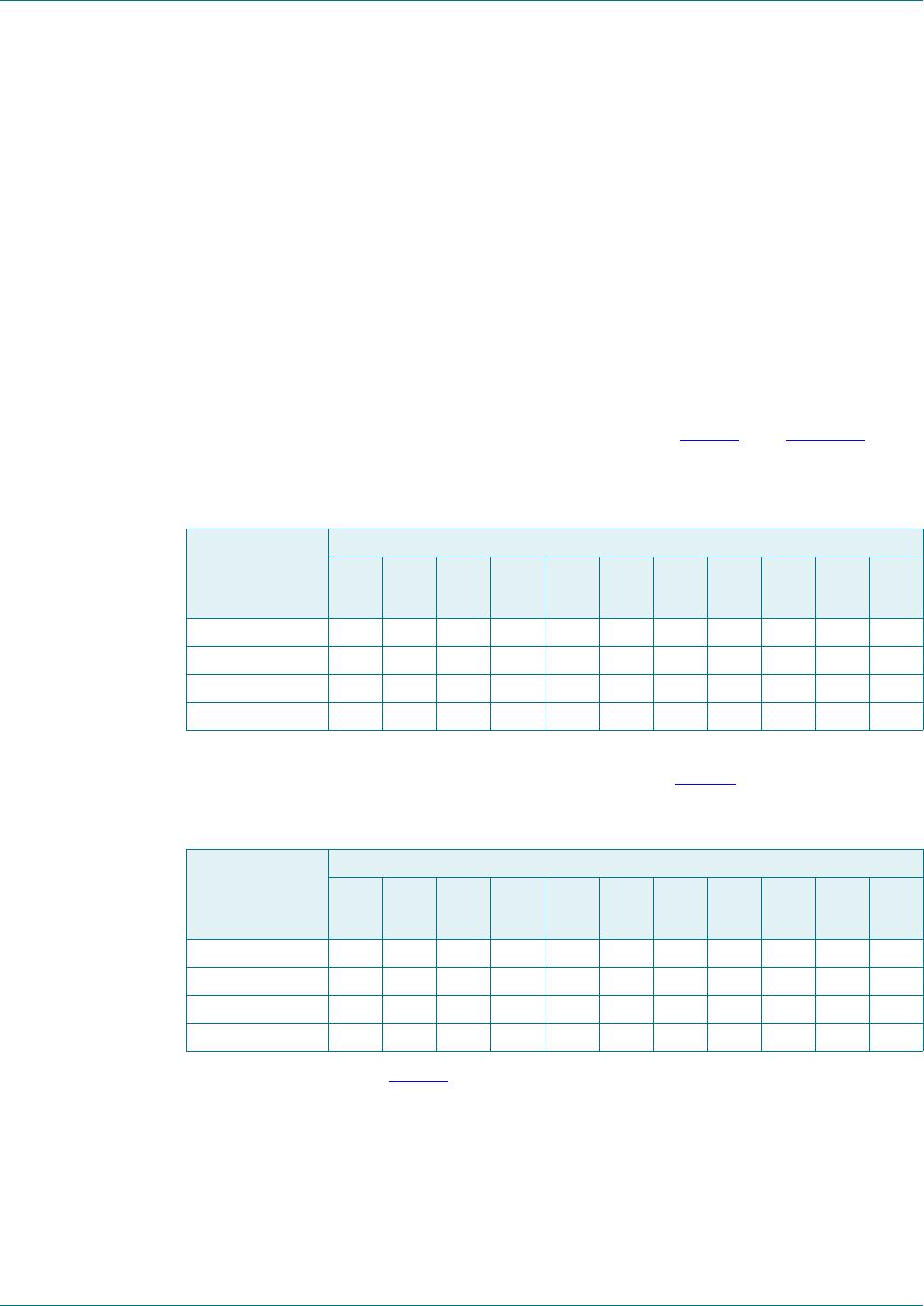
7.10.3 RAM writing in 1:3 multiplex drive mode
In 1:3 multiplex drive mode, the RAM is written as shown in Table 8 (see Figure 12 as
well).
If the bit at position BP2/S2 would be written by a second byte transmitted, then the
mapping of the segment bits would change as illustrated in Table 9
.
In the case described in Table 9 the RAM has to be written entirely and BP2/S2, BP2/S5,
BP2/S8 and so on, have to be connected to elements on the display. This can be
achieved by a combination of writing and rewriting the RAM like follows:
In the first write to the RAM, bits a7 to a0 are written.
In the second write, bits b7 to b0 are written, overwriting bits a1 and a0 with bits b7
and b6.
In the third write, bits c7 to c0 are written, overwriting bits b1 and b0 with bits c7 and
c6.
Table 8. Standard RAM filling in 1:3 multiplex drive mode
Assumption: BP2/S2, BP2/S5, BP2/S8 etc. are not connected to any elements on the display.
Display RAM
bits (rows)/
backplane
outputs (BPn)
Display RAM addresses (columns)/segment outputs (Sn)
0 1 2 3 4 5 6 7 8 9 :
0 a7 a4 a1 b7 b4 b1 c7 c4 c1 d7 :
1 a6 a3 a0 b6 b3 b0 c6 c3 c0 d6 :
2 a5 a2 - b5 b2 - c5 c2 - d5 :
3 ----------:
Table 9. Entire RAM filling by rewriting in 1:3 multiplex drive mode
Assumption: BP2/S2, BP2/S5, BP2/S8 etc. are connected to elements on the display.
Display RAM
bits (rows)/
backplane
outputs (BPn)
Display RAM addresses (columns)/segment outputs (Sn)
0 1 2 3 4 5 6 7 8 9 :
0 a7 a4 a1/b7 b4 b1/c7 c4 c1/d7 d4 d1/e7 e4 :
1 a6 a3 a0/b6 b3 b0/c6 c3 c0/d6 d3 d0/e6 e3 :
2 a5 a2 b5 b2 c5 c2 d5 d2 e5 e2 :
3 ----------:
PCA85134 All information provided in this document is subject to legal disclaimers. © NXP Semiconductors N.V. 2014. All rights reserved.
Product data sheet Rev. 2 — 6 May 2014 21 of 53
NXP Semiconductors
PCA85134
Automotive 60 x 4 LCD segment driver for low multiplex rates
Depending on the method of writing to the RAM (standard or entire filling by rewriting),
some elements remain unused or can be used. But it has to be considered in the module
layout process as well as in the driver software design.
7.10.4 Bank selector
7.10.4.1 Output bank selector
The output bank selector (see Table 15
) selects one of the four rows per display RAM
address for transfer to the display register. The actual row selected depends on the
particular LCD drive mode in operation and on the instant in the multiplex sequence.
In 1:4 multiplex mode, all RAM addresses of row 0 are selected, these are followed by
the contents of row 1, 2, and then 3
In 1:3 multiplex mode, rows 0, 1, and 2 are selected sequentially
In 1:2 multiplex mode, rows 0 and 1 are selected
In static mode, row 0 is selected
The SYNC
signal resets these sequences to the following starting points:
row 3 for 1:4 multiplex
row 2 for 1:3 multiplex
row 1 for 1:2 multiplex
row 0 for static mode
The PCA85134 includes a RAM bank switching feature in the static and 1:2 multiplex
drive modes. In the static drive mode, the bank-select command may request the contents
of row 2 to be selected for display instead of the contents of row 0. In the 1:2 multiplex
mode, the contents of rows 2 and 3 may be selected instead of rows 0 and 1. This gives
the provision for preparing display information in an alternative bank and to be able to
switch to it once it is assembled.
7.10.4.2 Input bank selector
The input bank selector loads display data into the display data in accordance with the
selected LCD drive configuration. Display data can be loaded in row 2 in static drive mode
or in rows 2 and 3 in 1:2 multiplex drive mode by using the bank-select command (see
Table 15
). The input bank selector functions independently to the output bank selector.
7.11 Blinking
The display blinking capabilities of the PCA85134 are very versatile. The whole display
can blink at frequencies selected by the blink-select command (see Table 16
). The blink
frequencies are derived from the clock frequency. The ratio between the clock and blink
frequency depends on the blink mode selected (see Table 10
).

PCA85134H/Q900/1,1

Mfr. #:
Manufacturer:
NXP Semiconductors
Description:
LCD Drivers 60 X 4 LCD DRIVER FOR MULTIPLEX RATES
Lifecycle:
New from this manufacturer.
Delivery:
DHL FedEx Ups TNT EMS
Payment:
T/T Paypal Visa MoneyGram Western Union

Products related to this Datasheet