PCA85134 All information provided in this document is subject to legal disclaimers. © NXP Semiconductors N.V. 2014. All rights reserved.
Product data sheet Rev. 2 — 6 May 2014 34 of 53
NXP Semiconductors
PCA85134
Automotive 60 x 4 LCD segment driver for low multiplex rates
13. Dynamic characteristics
Table 21. Dynamic characteristics
V
DD
= 1.8 V to 5.5 V; V
SS
= 0 V; V
LCD
= 2.5 V to 8.0 V; T
amb
=
40
C to +95
C; unless otherwise specified.
Symbol Parameter Conditions Min Typ Max Unit
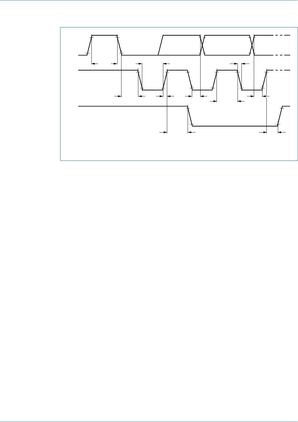
Clock
Internal: output pin CLK
f
osc
oscillator frequency V
DD
= 5 V
[1]
1440 1970 2640 Hz
External: input pin CLK
f
clk(ext)
external clock
frequency
V
DD
= 5 V 800 - 3600 Hz
t
clk(H)
HIGH-level clock time 130 - - s
t
clk(L)
LOW-level clock time 130 - - s
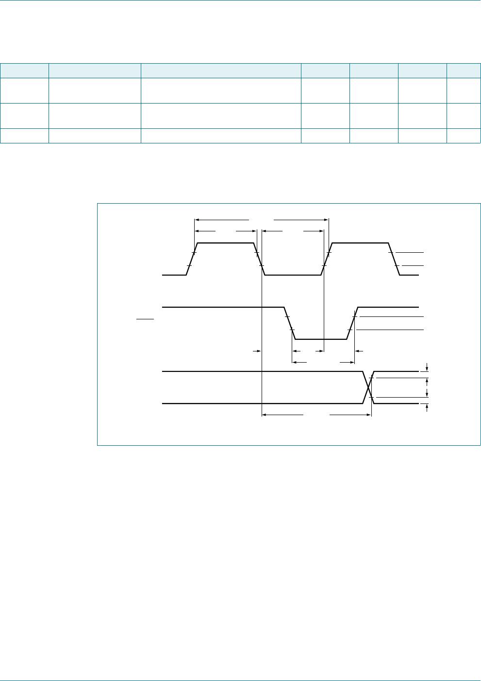
Synchronization: input pin SYNC
t
PD(SYNC_N)
SYNC propagation
delay
-30-ns
t
SYNC_NL
SYNC LOW time 1 - - s
Outputs: pins BP0 to BP3 and S0 to S59
t
PD(drv)
driver propagation
delay
V
LCD
= 5 V - - 30 s
I
2
C-bus: timing
[2]
Pin SCL
f
SCL
SCL frequency - - 400 kHz
t
LOW
LOW period of the
SCL clock
1.3 - - s
t
HIGH
HIGH period of the
SCL clock
0.6 - - s
Pin SDA
t
SU;DAT
data set-up time 100 - - ns
t
HD;DAT
data hold time 0 - - ns
Pins SCL and SDA
t
BUF
bus free time between
a STOP and START
condition
1.3 - - s
t
SU;STO
set-up time for STOP
condition
0.6 - - s
t
HD;STA
hold time (repeated)
START condition
0.6 - - s
t
SU;STA
set-up time for a
repeated START
condition
0.6 - - s
t
r
rise time of both SDA
and SCL signals
f
SCL
= 400 kHz - - 0.3 s
f
SCL
= 100 kHz - - 1.0 s