PCA85134 All information provided in this document is subject to legal disclaimers. © NXP Semiconductors N.V. 2014. All rights reserved.
Product data sheet Rev. 2 — 6 May 2014 27 of 53
NXP Semiconductors
PCA85134
Automotive 60 x 4 LCD segment driver for low multiplex rates
8.4 I
2
C-bus controller
The PCA85134 acts as an I
2
C-bus slave receiver. It does not initiate I
2
C-bus transfers or
transmit data to an I
2
C-bus master receiver. The only data output from the PCA85134 are
the acknowledge signals of the selected devices. Device selection depends on the
I
2
C-bus slave address, on the transferred command data and on the hardware
subaddress.
In single device applications, the hardware subaddress inputs A0, A1, and A2 are
normally tied to V
SS
which defines the hardware subaddress 0. In multiple device
applications A0, A1, and A2 are tied to V
SS
or V
DD
using a binary coding scheme, so that
no two devices with a common I
2
C-bus slave address have the same hardware
subaddress.
8.5 Input filters
To enhance noise immunity in electrically adverse environments, RC low-pass filters are
provided on the SDA and SCL lines.
8.6 I
2
C-bus protocol
Two I
2
C-bus slave addresses (0111 000 and 0111 001) are used to address the
PCA85134. The entire I
2
C-bus slave address byte is shown in Table 17.
The PCA85134 is a write-only device and does not respond to a read access, therefore
bit 0 should always be logic 0. Bit 1 of the slave address byte, that a PCA85134 will
respond to, is defined by the level tied to its SA0 input (V
SS
for logic 0 and V
DD
for logic 1).
Having two reserved slave addresses allows the following on the same I
2
C-bus:
• Up to 16 PCA85134 for very large LCD applications
• The use of two types of LCD multiplex drive
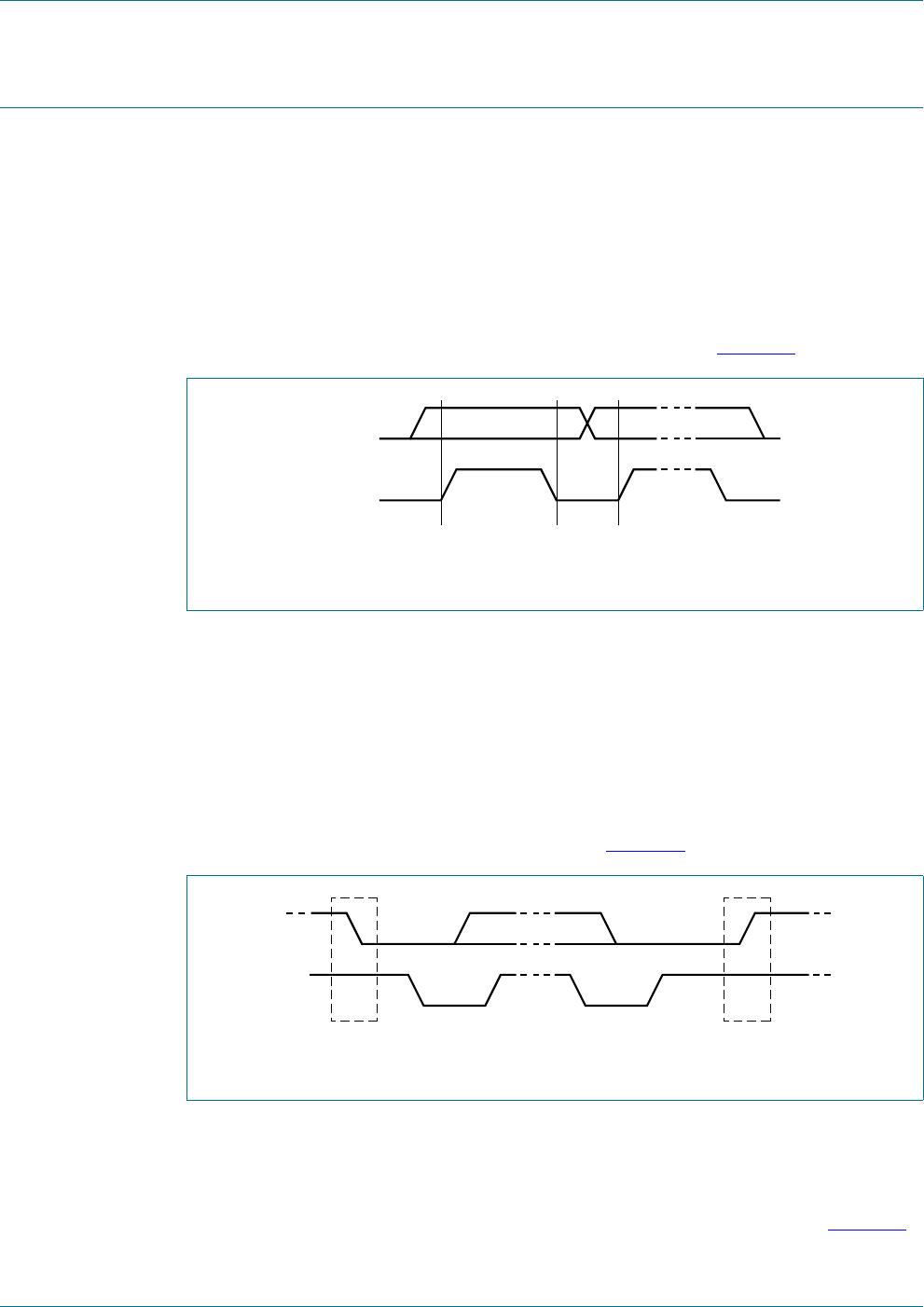
The I
2
C-bus protocol is shown in Figure 17. The sequence is initiated with a START
condition (S) from the I
2
C-bus master which is followed by one of the available PCA85134
slave addresses. All PCA85134 with the same SA0 level acknowledge in parallel to the
slave address. All PCA85134 with the alternative SA0 level ignore the whole I
2
C-bus
transfer.
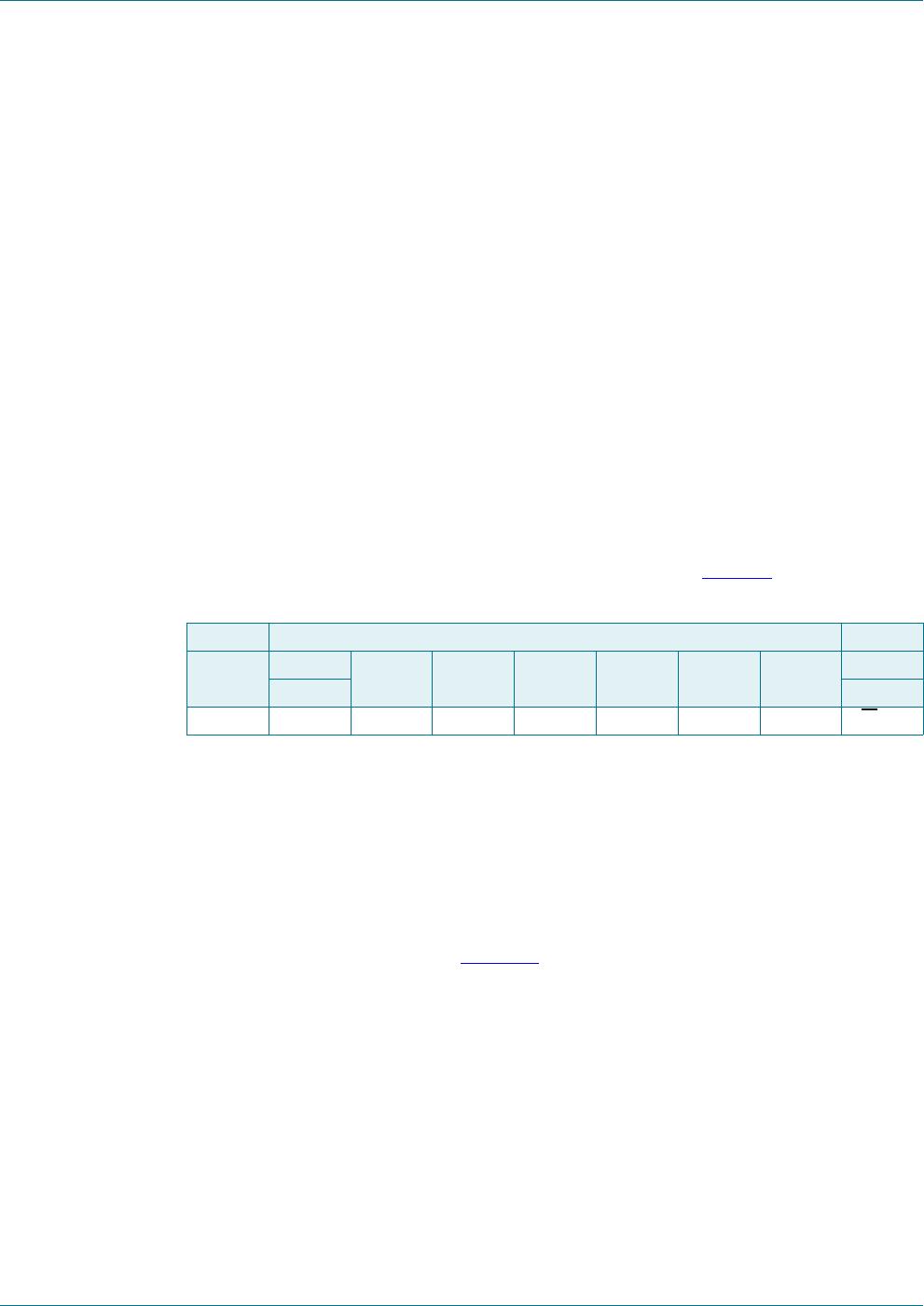
Table 17. I
2
C slave address byte
Slave address
Bit 7 6 5 4 3 2 1 0
MSB LSB
011100SA0R/W