PCA85134 All information provided in this document is subject to legal disclaimers. © NXP Semiconductors N.V. 2014. All rights reserved.
Product data sheet Rev. 2 — 6 May 2014 5 of 53
NXP Semiconductors
PCA85134
Automotive 60 x 4 LCD segment driver for low multiplex rates
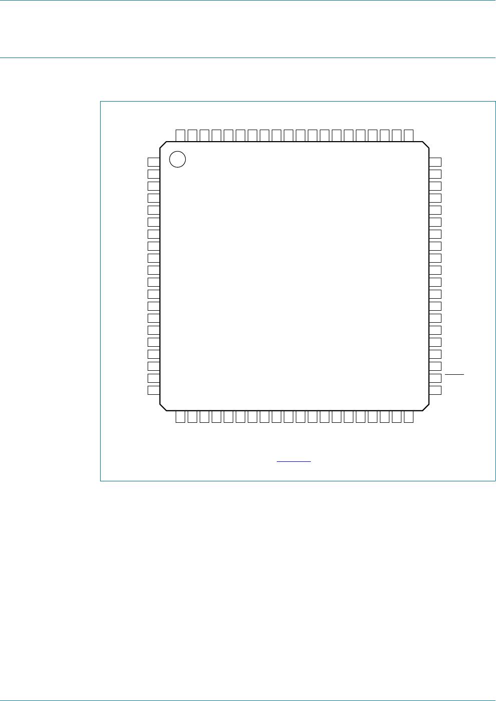
6.2 Pin description
Table 4. Pin description
Input or input/output pins must always be at a defined level (V
SS
or V
DD
) unless otherwise specified.
Symbol Pin Type Description
S31 to S59 1 to 29 output LCD segment output 31 to 59
BP0 to BP3 30 to 33 output LCD backplane output 0 to 3
n.c. 34 to 37 - not connected; do not connect and do not use as
feed through
SDA 38 input/output I
2
C-bus serial data input and output
SCL 39 input I
2
C-bus serial clock input
CLK 40 input/output external clock input and internal clock output
V
DD
41 supply supply voltage
SYNC
42 input/output cascade synchronization input and output (active
LOW)
OSC 43 input enable input for internal oscillator
A0 to A2 44 to 46 input subaddress counter input 0 to 2
SA0 47 input I
2
C-bus slave address input 0
V
SS
48 supply ground supply voltage
V
LCD
49 supply input of LCD supply voltage
S0 to S30 50 to 80 output LCD segment output 0 to 30