PCA85134 All information provided in this document is subject to legal disclaimers. © NXP Semiconductors N.V. 2014. All rights reserved.
Product data sheet Rev. 2 — 6 May 2014 24 of 53
NXP Semiconductors
PCA85134
Automotive 60 x 4 LCD segment driver for low multiplex rates
[1] The bank-select command has no effect in 1:3 or 1:4 multiplex drive modes.
[2] Default value.
[1] Default value.
[2] Normal blinking is assumed when the LCD multiplex drive modes 1:3 or 1:4 are selected.
[3] Alternate RAM bank blinking does not apply in 1:3 and 1:4 multiplex drive modes.
[4] For the blink frequencies, see Table 10
.
7.13 Display controller
The display controller executes the commands identified by the command decoder. It
contains the status registers of the PCA85134 and coordinates their effects. The display
controller is also responsible for loading display data into the display RAM in the correct
filling order.
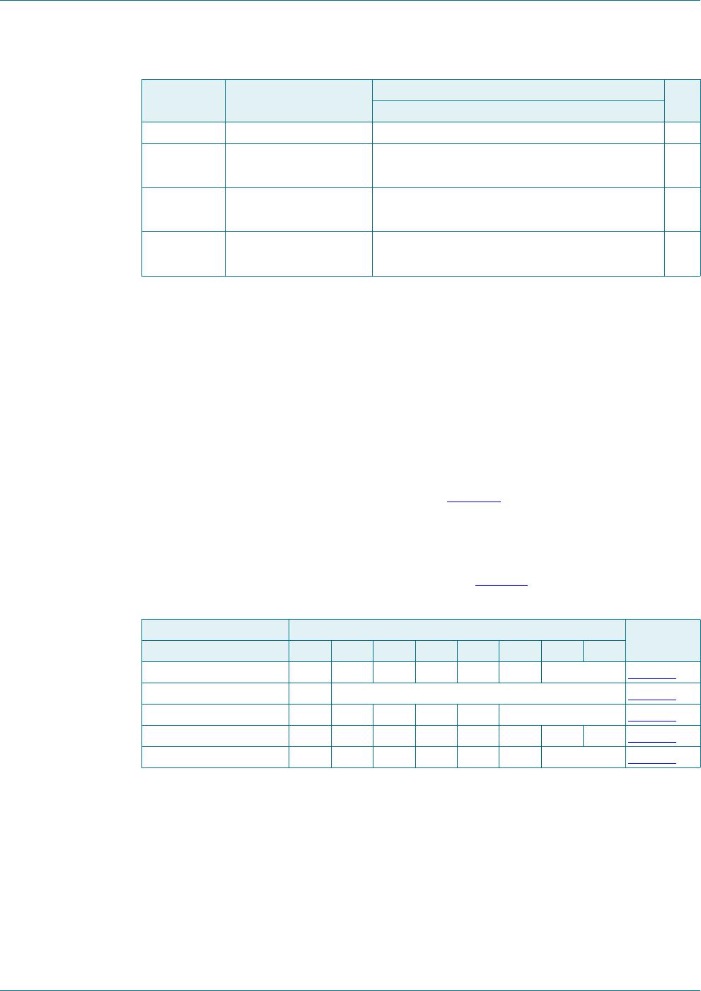
Table 15. Bank-select command bit description
See Section 7.10.4 on page 21.
Bit Symbol Value Description
Static 1:2 multiplex
[1]
7 to 2 - 111110 fixed value
1I input bank selection: storage of arriving
display data
0
[2]
RAM row 0 RAM rows 0 and 1
1 RAM row 2 RAM rows 2 and 3
0O output bank selection: retrieval of LCD display
data
0
[2]
RAM row 0 RAM rows 0 and 1
1 RAM row 2 RAM rows 2 and 3
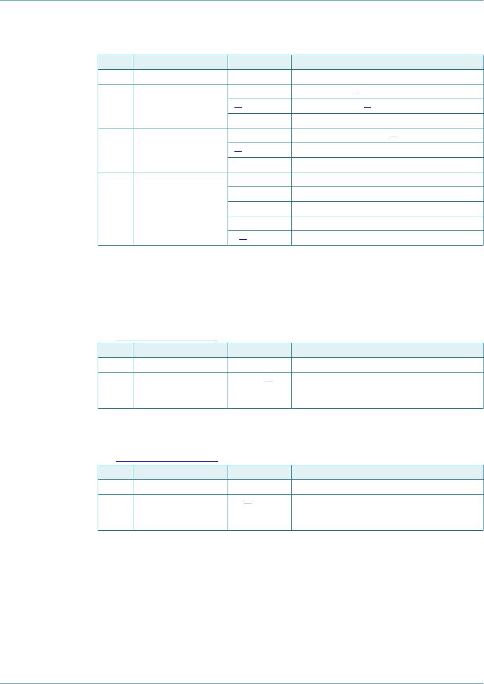
Table 16. Blink-select command bit description
See Section 7.11 on page 21
.
Bit Symbol Value Description
7 to 3 - 11110 fixed value
2AB blink mode selection
0
[1]
normal blinking
[2]
1 alternate RAM bank blinking
[3]
1 to 0 BF[1:0] blink frequency selection
[4]
00
[1]
off
01 1
10 2
11 3