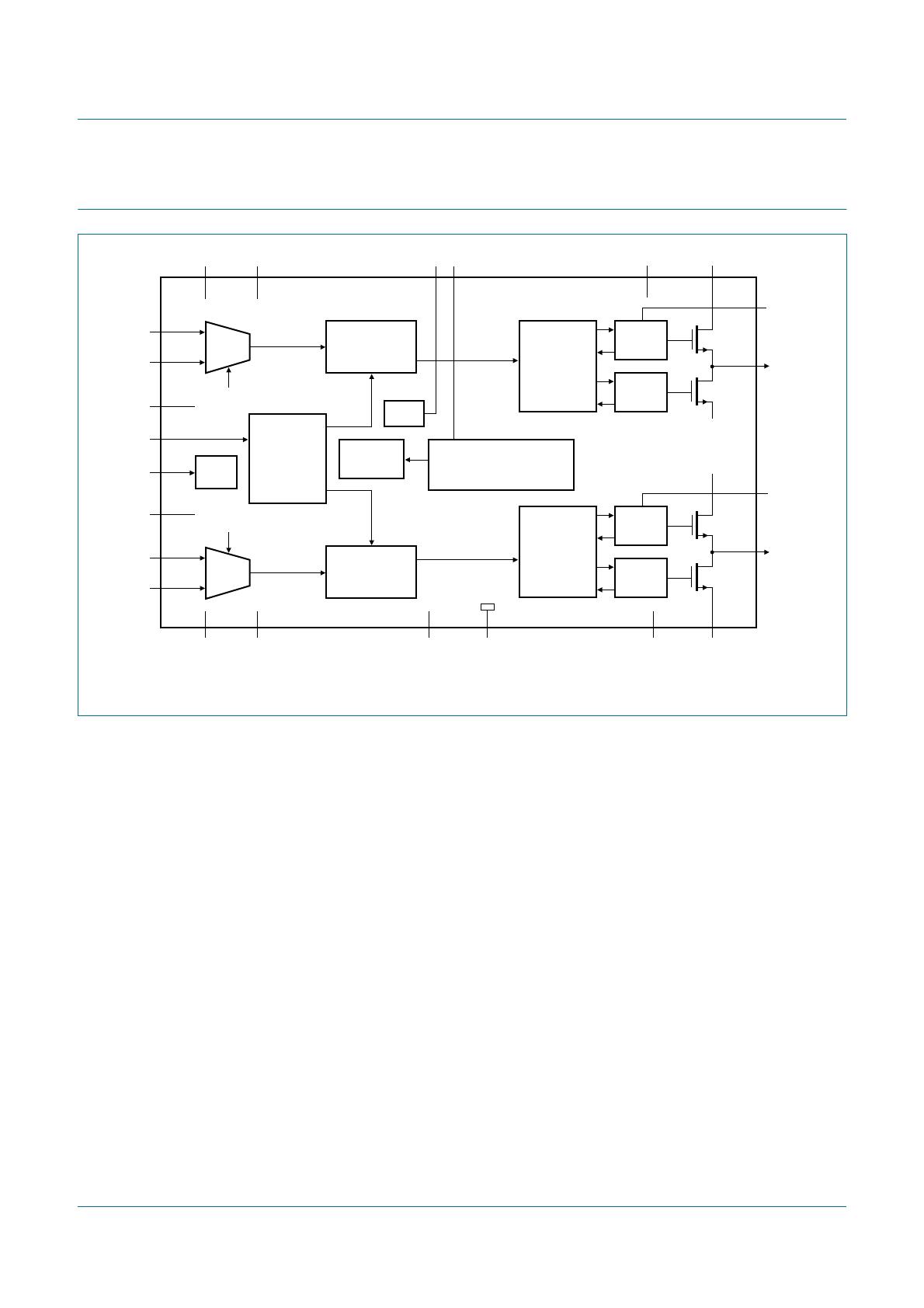
1. General description
The TDA8920C is a high-efficiency class-D audio power amplifier. The typical output
power is 2 × 110 W with a speaker load impedance of 4 .
The TDA8920C is available in both HSOP24 and DBS23P power packages. The amplifier
operates over a wide supply voltage range from ±12.5 V to ±32.5 V and features low
quiescent current consumption.
2. Features
n Pin compatible with TDA8950/20B for both HSOP24 and DBS23P packages
n Symmetrical operating supply voltage range from ±12.5 V to ±32.5 V
n Stereo full differential inputs, can be used as stereo Single-Ended (SE) or mono
Bridge-Tied Load (BTL) amplifier
n High output power in typical applications:
u SE 2 × 110 W, R
L
=4 (V
P
= ±30 V)
u SE 2 × 125 W, R
L
=4 (V
P
= ±32 V)
u SE 2 × 120 W, R
L
=3 (V
P
= ±29 V)
u BTL 1 × 220 W, R
L
=8 (V
P
= ±30 V)
n Low noise
n Smooth pop noise-free start-up and switch off
n Zero dead time switching
n Fixed frequency
n Internal or external clock
n High efficiency
n Low quiescent current
n Advanced protection strategy: voltage protection and output current limiting
n Thermal FoldBack (TFB)
n Fixed gain of 30 dB in SE and 36 dB in BTL applications
n Fully short-circuit proof across load
n BD modulation in BTL configuration
3. Applications
n DVD
n Mini and micro receiver
n Home Theater In A Box (HTIAB) system
n High-power speaker system
TDA8920C
2 × 110 W class-D power amplifier
Rev. 02 — 11 June 2009 Product data sheet
TDA8920C_2 © NXP B.V. 2009. All rights reserved.
Product data sheet Rev. 02 — 11 June 2009 2 of 39
NXP Semiconductors
TDA8920C
2 × 110 W class-D power amplifier
4. Quick reference data
[1] V
P
is the supply voltage on pins VDDP1, VDDP2 and VDDA.
[2] The circuit is DC adjusted at V
P
= ±12.5 V to ±32.5 V.
[3] Output power is measured indirectly; based on R
DSon
measurement; see Section 13.3.
5. Ordering information
Table 1. Quick reference data
Symbol Parameter Conditions Min Typ Max Unit
General, V
P
[1]
= ±30 V
V
P
supply voltage Operating mode
[2]
±12.5 ±30 ±32.5 V
V
P(ovp)
overvoltage protection supply voltage Standby, Mute modes; V
DD
V
SS
65 - 70 V
I
q(tot)
total quiescent current Operating mode; no load; no filter; no
RC-snubber network connected
-5075mA
Stereo single-ended configuration
P
o
output power T
j
=85°C; L
LC
=22µH; C
LC
= 680 nF
(see
Figure 10)
THD + N = 10 %; R
L
=4;
V
P
= ±30 V
[3]
- 110 - W
THD + N = 10 %; R
L
=4;
V
P
= ±27 V
-90- W
Mono bridge-tied load configuration
P
o
output power T
j
=85°C; L
LC
=22µH; C
LC
= 680 nF
(see
Figure 10); R
L
=8;
THD + N = 10 %; V
P
= ±30 V
[3]
- 220 - W
Table 2. Ordering information
Type number Package
Name Description Version
TDA8920CJ DBS23P plastic DIL-bent-SIL power package; 23 leads (straight lead length 3.2 mm) SOT411-1
TDA8920CTH HSOP24 plastic, heatsink small outline package; 24 leads; low stand-off height SOT566-3
TDA8920C_2 © NXP B.V. 2009. All rights reserved.
Product data sheet Rev. 02 — 11 June 2009 3 of 39
NXP Semiconductors
TDA8920C
2 × 110 W class-D power amplifier
6. Block diagram
Pin numbers in brackets refer to type number TDA8920CJ.
Fig 1. Block diagram
001aai852
OUT1
V
SSP1
V
DDP2
DRIVER
HIGH
OUT2
BOOT2
TDA8920CTH
(TDA8920CJ)
BOOT1
DRIVER
LOW
SWITCH1
CONTROL
AND
HANDSHAKE
PWM
MODULATOR
MANAGER
OSCILLATOR
TEMPERATURE SENSOR
CURRENT PROTECTION
VOLTAGE PROTECTION
STABI
MODE
INPUT
STAGE
mute
9 (3)
8 (2)
IN1M
IN1P
22 (15)
21 (14)
20 (13)
17 (11)
16 (10)
15 (9)
VSSP2VSSP1
DRIVER
HIGH
DRIVER
LOW
SWITCH2
CONTROL
AND
HANDSHAKE
PWM
MODULATOR
11 (5)
n.c.
7 (1)
OSC
2 (19)
SGND
6 (23)
MODE
INPUT
STAGE
mute
5 (22)
4 (21)
IN2M
IN2P
19 (-)24 (17)
VSSD n.c.
1 (18)
VSSA
12 (6)
n.c.
3 (20)
VDDA
10 (4)
n.c.
23 (16)13 (7)18 (12) 14 (8)
VDDP2
PROTSTABI
VDDP1

TDA8920CJ/N1,112

Mfr. #:
Manufacturer:
NXP Semiconductors
Description:
Audio Amplifiers Audio Amp Speaker 1CH Mono/2-CH Stereo
Lifecycle:
New from this manufacturer.
Delivery:
DHL FedEx Ups TNT EMS
Payment:
T/T Paypal Visa MoneyGram Western Union

Products related to this Datasheet