TDA8920C_2 © NXP B.V. 2009. All rights reserved.
Product data sheet Rev. 02 — 11 June 2009 34 of 39
NXP Semiconductors
TDA8920C
2 × 110 W class-D power amplifier
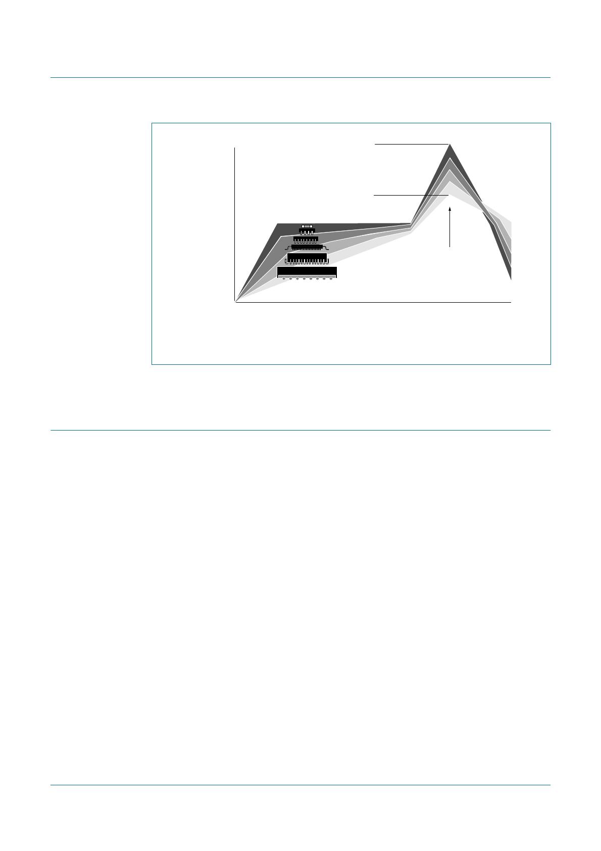
15. Soldering of SMD packages
This text provides a very brief insight into a complex technology. A more in-depth account
of soldering ICs can be found in Application Note
AN10365 “Surface mount reflow
soldering description”
.
15.1 Introduction to soldering
Soldering is one of the most common methods through which packages are attached to
Printed Circuit Boards (PCBs), to form electrical circuits. The soldered joint provides both
the mechanical and the electrical connection. There is no single soldering method that is
ideal for all IC packages. Wave soldering is often preferred when through-hole and
Surface Mount Devices (SMDs) are mixed on one printed wiring board; however, it is not
suitable for fine pitch SMDs. Reflow soldering is ideal for the small pitches and high
densities that come with increased miniaturization.
15.2 Wave and reflow soldering
Wave soldering is a joining technology in which the joints are made by solder coming from
a standing wave of liquid solder. The wave soldering process is suitable for the following:
Through-hole components
Leaded or leadless SMDs, which are glued to the surface of the printed circuit board
Not all SMDs can be wave soldered. Packages with solder balls, and some leadless
packages which have solder lands underneath the body, cannot be wave soldered. Also,
leaded SMDs with leads having a pitch smaller than ~0.6 mm cannot be wave soldered,
due to an increased probability of bridging.
The reflow soldering process involves applying solder paste to a board, followed by
component placement and exposure to a temperature profile. Leaded packages,
packages with solder balls, and leadless packages are all reflow solderable.
Key characteristics in both wave and reflow soldering are:
Board specifications, including the board finish, solder masks and vias
Package footprints, including solder thieves and orientation
The moisture sensitivity level of the packages
Package placement
Inspection and repair
Lead-free soldering versus SnPb soldering
15.3 Wave soldering
Key characteristics in wave soldering are:
Process issues, such as application of adhesive and flux, clinching of leads, board
transport, the solder wave parameters, and the time during which components are
exposed to the wave
Solder bath specifications, including temperature and impurities
TDA8920C_2 © NXP B.V. 2009. All rights reserved.
Product data sheet Rev. 02 — 11 June 2009 35 of 39
NXP Semiconductors
TDA8920C
2 × 110 W class-D power amplifier
15.4 Reflow soldering
Key characteristics in reflow soldering are:
Lead-free versus SnPb soldering; note that a lead-free reflow process usually leads to
higher minimum peak temperatures (see Figure 30) than a SnPb process, thus
reducing the process window
Solder paste printing issues including smearing, release, and adjusting the process
window for a mix of large and small components on one board
Reflow temperature profile; this profile includes preheat, reflow (in which the board is
heated to the peak temperature) and cooling down. It is imperative that the peak
temperature is high enough for the solder to make reliable solder joints (a solder paste
characteristic). In addition, the peak temperature must be low enough that the
packages and/or boards are not damaged. The peak temperature of the package
depends on package thickness and volume and is classified in accordance with
Table 12 and 13
Moisture sensitivity precautions, as indicated on the packing, must be respected at all
times.
Studies have shown that small packages reach higher temperatures during reflow
soldering, see Figure 30.
Table 12. SnPb eutectic process (from J-STD-020C)
Package thickness (mm) Package reflow temperature (°C)
Volume (mm
3
)
< 350 350
< 2.5 235 220
2.5 220 220
Table 13. Lead-free process (from J-STD-020C)
Package thickness (mm) Package reflow temperature (°C)
Volume (mm
3
)
< 350 350 to 2000 > 2000
< 1.6 260 260 260
1.6 to 2.5 260 250 245
> 2.5 250 245 245
TDA8920C_2 © NXP B.V. 2009. All rights reserved.
Product data sheet Rev. 02 — 11 June 2009 36 of 39
NXP Semiconductors
TDA8920C
2 × 110 W class-D power amplifier
For further information on temperature profiles, refer to Application Note
AN10365
“Surface mount reflow soldering description”
.
16. Soldering of through-hole mount packages
16.1 Introduction to soldering through-hole mount packages
This text gives a very brief insight into wave, dip and manual soldering.
Wave soldering is the preferred method for mounting of through-hole mount IC packages
on a printed-circuit board.
16.2 Soldering by dipping or by solder wave
Driven by legislation and environmental forces the worldwide use of lead-free solder
pastes is increasing. Typical dwell time of the leads in the wave ranges from
3 seconds to 4 seconds at 250 °C or 265 °C, depending on solder material applied, SnPb
or Pb-free respectively.
The total contact time of successive solder waves must not exceed 5 seconds.
The device may be mounted up to the seating plane, but the temperature of the plastic
body must not exceed the specified maximum storage temperature (T
stg(max)
). If the
printed-circuit board has been pre-heated, forced cooling may be necessary immediately
after soldering to keep the temperature within the permissible limit.
16.3 Manual soldering
Apply the soldering iron (24 V or less) to the lead(s) of the package, either below the
seating plane or not more than 2 mm above it. If the temperature of the soldering iron bit is
less than 300 °C it may remain in contact for up to 10 seconds. If the bit temperature is
between 300 °C and 400 °C, contact may be up to 5 seconds.
MSL: Moisture Sensitivity Level
Fig 30. Temperature profiles for large and small components
001aac844
temperature
time
minimum peak temperature
= minimum soldering temperature
maximum peak temperature
= MSL limit, damage level
peak
temperature

TDA8920CJ/N1,112

Mfr. #:
Manufacturer:
NXP Semiconductors
Description:
Audio Amplifiers Audio Amp Speaker 1CH Mono/2-CH Stereo
Lifecycle:
New from this manufacturer.
Delivery:
DHL FedEx Ups TNT EMS
Payment:
T/T Paypal Visa MoneyGram Western Union

Products related to this Datasheet