TDA8920C_2 © NXP B.V. 2009. All rights reserved.
Product data sheet Rev. 02 — 11 June 2009 10 of 39
NXP Semiconductors
TDA8920C
2 × 110 W class-D power amplifier
When OCP is activated, the power transistors are turned off. They are turned on again
during the next switching cycle. If the output current is still greater than the OCP threshold,
they will be immediately switched off again. This switching will continue until C
PROT
is fully
discharged. The amplifier will then be switched off completely and a restart sequence
initiated.
After a fixed period of 100 ms, the amplifier will attempt to switch on again, but will fail if
the output current still exceeds the OCP threshold. The amplifier will continue trying to
switch on every 100 ms. The average power dissipation will be low in this situation
because the duty cycle is low.
Switching the amplifier on and off in this way will generate unwanted ‘audio holes’. This
can be avoided by increasing the value of C
PROT
(up to 220 pF) to delay amplifier
switch-off. C
PROT
will also prevent the amplifier switching off due to transient
frequency-dependent impedance drops at the speakers.
The amplifier will switch on, and remain in Operating mode, once the overcurrent
condition has been removed. OCP ensures the TDA8920C amplifier is fully protected
against short-circuit conditions while avoiding audio holes.
[1] OVP can be triggered by supply pumping; see Section 13.6.
8.3.3 Window Protection (WP)
Window Protection (WP) checks the conditions at the output terminals of the power stage
and is activated:
During the start-up sequence, when the TDA8920C is switching from Standby to
Mute.
Start-up will be interrupted If a short-circuit is detected between one of the output
terminals and pin VDDP1/VDDP2 or VSSP1/VSSP2. The TDA8920C will wait until the
short-circuit to the supply lines has been removed before resuming start-up. The short
circuit will not generate large currents because the short-circuit check is carried out
before the power stages are enabled.
When the amplifier is shut down completely because the OCP circuit has detected a
short circuit to one of the supply lines.
WP will be activated when the amplifier attempts to restart after 100 ms (see
Section 8.3.2). The amplifier will not start-up again until the short circuit to the supply
lines has been removed.
Table 4. Current limiting behavior during low output impedance conditions at different
values of C
PROT
Type V
P
(V)
V
I
(mV, p-p) f (Hz) C
PROT
(pF)
PWM output stops
Short
(Z
th
=0)
Short
(Z
th
= 0.5 )
Short
(Z
th
=1)
TDA8920C 29.5 500 20 10 yes yes OVP
[1]
1000 10 yes yes no
20 15 yes yes OVP
[1]
1000 15 yes no no
1000 220 no no no
TDA8920C_2 © NXP B.V. 2009. All rights reserved.
Product data sheet Rev. 02 — 11 June 2009 11 of 39
NXP Semiconductors
TDA8920C
2 × 110 W class-D power amplifier
8.3.4 Supply voltage protection
If the supply voltage drops below the minimum supply voltage threshold, V
P(uvp)
, the UVP
circuit will be activated and the system will shut down. Once the supply voltage rises
above V
P(uvp)
again, the system will restart after a delay of 100 ms.
If the supply voltage exceeds the maximum supply voltage threshold, V
P(ovp)
, the OVP
circuit will be activated and the power stages will be shut down. When the supply voltage
drops below V
P(ovp)
again, the system will restart after a delay of 100 ms.
An additional UnBalance Protection (UBP) circuit compares the positive analog supply
voltage (on pin VDDA) with the negative analog supply voltage (on pin VSSA) and is
triggered if the voltage difference exceeds a factor of two (V
DDA
> 2 ×|V
SSA
| OR |V
SSA
| >
2 × V
DDA
). When the supply voltage difference drops below the unbalance threshold,
V
P(ubp)
, the system restarts after 100 ms.
An overview of all protection circuits and their respective effects on the output signal is
provided in Table 5.
[1] Amplifier gain depends on the junction temperature and heatsink size.
[2] The amplifier shuts down completely only if the short-circuit impedance is below the impedance threshold
(Z
th
; see Section 8.3.2). In all other cases, current limiting results in a clipped output signal.
[3] Fault condition detected during any Standby-to-Mute transition or during a restart after OCP has been
activated (short-circuit to one of the supply lines).
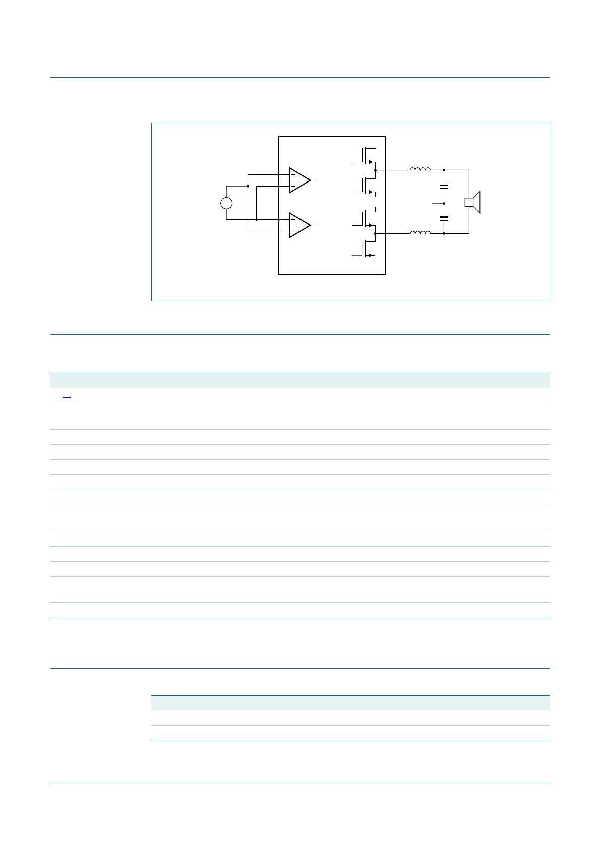
8.4 Differential audio inputs
The audio inputs are fully differential ensuring a high common mode rejection ratio and
maximum flexibility in the application.
Stereo operation: to avoid acoustical phase differences, the inputs should be in
antiphase and the speakers should be connected in antiphase. This configuration:
minimizes power supply peak current
minimizes supply pumping effects, especially at low audio frequencies
Mono BTL operation: the inputs must be connected in anti-parallel. The output of one
channel is inverted and the speaker load is connected between the two outputs of the
TDA8920C. In practice (because of the OCP threshold) the output power can be
boosted to twice the output power that can be achieved with the single-ended
configuration.
The input configuration for a mono BTL application is illustrated in Figure 7.
Table 5. Overview of TDA8920C protection circuits
Protection name Complete
shutdown
Restart directly Restart after
100 ms
Pin PROT
detection
TFB
[1]
NNNN
OTP Y N Y N
OCP Y
[2]
N
[2]
Y
[2]
Y
WP N
[3]
YNN
UVPYNYN
OVP Y N Y N
UBPYNYN
TDA8920C_2 © NXP B.V. 2009. All rights reserved.
Product data sheet Rev. 02 — 11 June 2009 12 of 39
NXP Semiconductors
TDA8920C
2 × 110 W class-D power amplifier
9. Limiting values
[1] V
P
is the supply voltage on pins VDDP1, VDDP2 and VDDA.
10. Thermal characteristics
Fig 7. Input configuration for mono BTL application
V
in
IN1P
OUT1
power stage
mbl466
OUT2
SGND
IN1M
IN2P
IN2M
Table 6. Limiting values
In accordance with the Absolute Maximum Rating System (IEC 60134).
Symbol Parameter Conditions Min Max Unit
V
P
[1]
supply voltage Standby, Mute modes; V
DD
V
SS
-65 V
I
ORM
repetitive peak output current maximum output current limiting 9.2 - A
T
stg
storage temperature 55 +150 °C
T
amb
ambient temperature 40 +85 °C
T
j
junction temperature - 150 °C
V
MODE
voltage on pin MODE referenced to SGND 0 6 V
V
OSC
voltage on pin OSC 0 SGND + 6 V
V
I
input voltage referenced to SGND; pin IN1P; IN1M;
IN2P and IN2M
5+5 V
V
PROT
voltage on pin PROT referenced to voltage on pin VSSD 0 12 V
V
ESD
electrostatic discharge voltage Human Body Model (HBM) 2000 +2000 V
Charged Device Model (CDM) 500 +500 V
I
q(tot)
total quiescent current Operating mode; no load; no filter; no
RC-snubber network connected
-75 mA
V
PWM(p-p)
peak-to-peak PWM voltage on pins OUT1 and OUT2 - 120 V
Table 7. Thermal characteristics
Symbol Parameter Conditions Typ Unit
R
th(j-a)
thermal resistance from junction to ambient in free air 40 K/W
R
th(j-c)
thermal resistance from junction to case 1.1 K/W

TDA8920CJ/N1,112

Mfr. #:
Manufacturer:
NXP Semiconductors
Description:
Audio Amplifiers Audio Amp Speaker 1CH Mono/2-CH Stereo
Lifecycle:
New from this manufacturer.
Delivery:
DHL FedEx Ups TNT EMS
Payment:
T/T Paypal Visa MoneyGram Western Union

Products related to this Datasheet